
H. F. Mohamed, Changtai Xia, Qinglin Sai, Huiyuan Cui, Mingyan Pan, Hongji Qi. Growth and fundamentals of bulk β-Ga2O3 single crystals[J]. Journal of Semiconductors, 2019, 40(1): 011801
- Journal of Semiconductors
- Vol. 40, Issue 1, 011801 (2019)
Abstract
1. Introduction
Beta gallium oxide has attracted rapidly growing interest in the past decade and is considered a promising candidate for power device applications. Gallium oxide is a significant semiconductor oxide and has a large bandgap energy (~4.9 eV) with a decent mobility (~100 cm2/Vs), a high breakdown strength (8 MV/cm), and good thermal stability. It was first studied in the 1950s, and its crystal structure was determined by Geller (1960)[
2. Crystal structure of β-Ga2O3
We discuss the crystal structure and electronic band structure of β-Ga2O3 and summarize the main points. Gallium oxide has a melting point of approximately 1800 °C, and five polymorphs named α, β, γ, δ, and ε exist in nature depending strictly on the preparation conditions[
β-Ga2O3 has a wide bandgap of ~ 4.9 eV[
As noted by Geller[
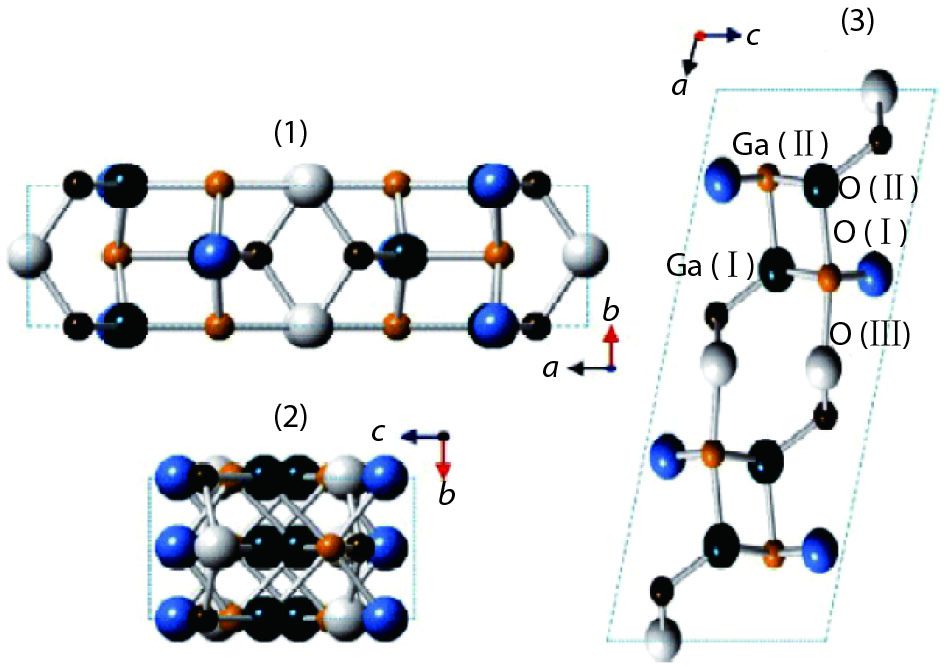
![]()
Figure 1.(Color online) Unit cell of
Thus far, the density functional theory (DFT) is the most suitable for calculating the electronic band structure of β-Ga2O3. Although, several theoretical studies on the electronic structure of β-Ga2O3 have been published[
![]()
Figure 2.(Color online) Electronic band structure of
3. Ga2O3 growth methods
In this section, we present an overview of the bulk crystal growth of β-Ga2O3. The following are the most common methods of bulk Ga2O3 crystal growth:
· Verneuil method
· Floating zone (FZ) method
· Czochralski (CZ) method
· Edge-defined film-fed growth (EFG) method
· Bridgman method
3.1. Verneuil method
The Verneuil method was developed by Auguste Verneuil in 1902 and is also known as flame fusion. This process is used mainly to fabricate the gem varieties of sapphire and ruby. The steps of the operation include melting the powder material using an oxyhydrogen flame, and thereafter, the melted material crystallizes into boule (as shown in Fig. 3).
![]()
Figure 3.(Color online) (a) Sketch of an early furnace used by Verneuil. (b) Simplified diagram of Verneuil process for synthesizing Ga2O3[
In 1964, Chase[
In addition, Lorenz et al.[
3.2. Floating zone (FZ) method
In 1955, Theurer[
![]()
Figure 4.(Color online) Schematic of float zone single crystal growth.
Villora et al.[
![]()
Figure 5.(Color online) As-grown crystals along the crystallographic axis (a- <100>), (b- <010>), (c- <001>]).
Moreover, Zhang et al. [
The major drawback of this method is that it is difficult to prevent the liquid from collapsing. It can only be held in place by surface tension. Cracks occur in the cooling crystal owing to the stress caused by high thermal gradients.
3.3. Czochralski method
The Czochralski method is a process of growing single crystals of metals (Pd, Pt, Ag, Au, etc.), semiconductors (Si, Ge, and GaAs), and artificial gemstones (Fig. 6).
![]()
Figure 6.Schematic of Czochralski method.
In 1915, Czochralski invented this method while investigating the rate of metal crystallization[
The diameter of the crystal increased to approximately 2 inch. The growth direction is always along the <010> crystallographic direction, which is parallel to both cleavage planes (100) and (001).
The first Czochralski growth of a β-Ga2O3 single crystal was reported by Tomm et al.[
![]()
Figure 7.(Color online) Semiconducting
Furthermore, the same co-workers of Galazka in 2018[
3.4. Edge-defined film-fed growth (EFG) method
Intensive experiments performed by La Belle and Mlavsky[
![]()
Figure 8.(Color online) Edge-defined film-fed growth method.
Kuramata et al.[
Chinese scientists also used this method to grow bulk crystals, Zhang et al.[
![]()
Figure 9.(Color online) (a) Photograph of EFG-grown
3.5. Bridgman method (vertical or horizontal)
The Bridgman–Stockbarger method is named after the Harvard physicist, Percy Williams Bridgman (1882–1961) and MIT physicist, Donald C. Stockbarger (1895–1952)[
![]()
Figure 10.(Color online) Bridgman technique.
Part of the seed will be re-melted after contact with the melt. One feature of this method of growing β-Ga2O3 is the utilization of a platinum–rhodium (70%–30%) crucible[
Hoshikawa et al.[
![]()
Figure 11.(Color online)
Ohba et al.[
![]()
Figure 12.(Color online) Schematics of line-shaped defects. The figure was adopted from Ref. [
In summary, the crucible-free FZ and Verneuil methods facilitate the use of a high oxygen concentration and a reduced amount of residual impurities. The Czochralski method provides a large crystal size of approximately 2 inch in diameter, while the EFG method provides a 6-inch-width crystal of the highest quality.
Ga2O3 substrates underwent a massive breakthrough owing to their low cost and low energy consumption. The following organization chart (Fig. 13) depicts the comparison of the melt growth methods for β-Ga2O3 bulk single crystals.
![]()
Figure 13.The comparison of the melt growth methods for
In addition, the best method for the mass production of substrates is the EFG method, which has a good track of the availability of large area, low defect density, high crystal quality.
4. Doping of β-Ga2O3
The conductivity control through doping and the curtailing of the trap states is the solution to obtaining β-Ga2O3 for technological applications[
4.1. Donor doping of β-Ga2O3
4.1.1. Unintentional self-doping
A β-Ga2O3 crystal exhibits n-type conductivity with no intentional doping. The n-type semiconductivity is commonly attributed to oxygen vacancies, which are ionized and form donors. Therefore, it is assumed that there is a strong correlation between the conductivity of β-Ga2O3 crystals and oxygen vacancies. This assumption has been debated by Varley et al.[
Zhang et al.[
4.1.2. Intentional n-type doping
The fabrication and characterization of Sn-doped β-Ga2O3 single crystals were studied by Suzuki et al.[
VÍllora et al.[
Sasaki et al.[
Zhou et al.[
4.2. Acceptor doping of β-Ga2O3
A major challenge for of β-Ga2O3 is its lack of an adequate method for fabricating p-type β-Ga2O3 crystals. Few reports on p-type Ga2O3 have been published[
4.2.1. Unintentional self-doping
Varley et al.[
4.2.2. Intentional p-type doping
Onuma et al.[
5. Applications
In this section, we present an overview of the applications of β-Ga2O3.
5.1. Gas sensors
The working principle of oxygen sensor devices is a negative relationship between the conductivity of β-Ga2O3 and the oxygen partial pressure in the surrounding atmosphere. The conductivity of the sensor changes with varying the proportion of oxygen or the concentration of gases in the atmosphere. Bartic et al.[
5.2. Power and high-voltage devices
The critical electric field can be determined from the bandgap using an empirical relationship[
Ec = 1.73 × 10⁵ (Eg)2.5
The estimated breakdown voltage is 8 MV/cm, which is approximately three times larger than that of SiC or GaN. The corresponding Baliga’s Fig. of merit (BFOM ∝ εμEc3), which is used to estimate the potential for power device applications, is at least four times larger than those of SiC or GaN. Furthermore, the conduction loss of Ga2O3 is lower than that of other semiconductor materials[
![]()
Figure 14.(Color online) Theoretical ideal performance limits of
5.3. Schottky diodes
High-performance Schottky barrier diodes were fabricated by Oishi et al.[
Recently, the highest performance of β-Ga2O3 Schottky barrier diode (SBD) was reported by Xidian University[
5.4. Field effect transistors (FET)
Higashiwaki et al.[
![]()
Figure 15.(Color online) Schematic illustration: (a) cross-section and (b) optical micrograph of Ga2O3 MESFET. According to the description from Ref. [
5.5. UV detectors
Photodetectors are one of the simplest devices to produce as they require only Schottky or Ohmic contacts. The major application of these devices is solar-blind ultraviolet (UV) radiation detection. Owing to its wide bandgap, Ga2O3 provides a unique opportunity for the detection of UV radiation of wavelengths <280 nm.
Suzuki et al.[
5.6. Radiation detection
Wide bandgap semiconductors feature strong bonds that provide them with an intrinsically high radiation resistance[
6. Conclusions and future perspectives
This review summaries the state of the art of β-Ga2O3 and achievements with respect to β-Ga2O3 ranging from preparation and characterization to applications. Although significant progress has been made in the growth of bulk crystals, defect and impurity control require further studies. As can be observed from this article, the published data on Ga2O3 are still incomplete and controversial to some extent. We look forward to realizing the following objectives that may be important research and development paths with respect to β-Ga2O3 bulk-based devices.
(1) Identification of the dominant defects in bulk crystals and their effect on device performance
(2) Experimental efforts to address open issues such as p-type conductivity and realizing the full potential of Ga2O3 materials in device applications
(3) New concepts and designs for improving the thermal management and reliability of power electronics devices
(4) Further progress in growth of large-diameter high-quality crystals
Acknowledgments
This work is funded by the following grants: Chinese Academy of Sciences president’s International Fellowship Initiative (Grant No. 2018PE0033), National Natural Science Foundation of China (Grant No. 51802327), Science and Technology Commission of Shanghai Municipality (No. 18511110500), and Pre-research Fund Key Project (No. 6140922010601) .
References
[1] S Geller. Crystal structure of β-Ga2O3. J Chem Phys, 33, 676(1960).
[2] R Roy, V G Hill, E F J Osborn. Polymorphism of Ga2O3 and the System Ga2O3−H2O. Am Chem Soc, 74, 719(1952).
[3] H H Tippins. Optical absorption and photoconductivity in the band edge of β−Ga2O3. Phys Rev, 140, A316(1965).
[4] Z Hajnal, J Miro, G Kiss et al. Role of oxygen vacancy defect states in the n-type conduction of β-Ga2O3. J Appl Phys, 86, 3792(1999).
[5] J A Kohn, G Katz, J D Broder. Characterization of β-Ga2O3 and its alumina Isomorph θ-Al2O3. Am Minerol, 42, 398(1956).
[6] G M Wolten, A B Chase. Determination of the point group of β-Ga2O3 from morphology and physical properties. J Solid State Chem, 16, 377(1976).
[7] J Ahman, G mSvensson, J Albertsson. A reinvestigation of β-gallium oxide. Acta Crystallogr Sect C Cryst Struct Commun, 52, 1336(1996).
[8] C Janowitz, V Scherer, M Mohamed et al. Experimental electronic structure of In2O3 and Ga2O3. New J Phys, 13, 085014(2011).
[9] S Yoshioka, H Hayashi, A Kuwabara et al. Structures and energetics of Ga2O3 polymorphs. J Phys Condens Matter, 19, 346211(2007).
[10] K Yamaguchi. First principles study on electronic structure of β-Ga2O3. Solid State Commun, 131, 739(2004).
[11] H He, R Orlando, M Blanco et al. First-principles study of the structural, electronic, and optical properties of Ga2O3 in its monoclinic and hexagonal phases. Phys Rev B, 74, 195123(2006).
[12] Y Zhang, J Yan, G Zhao et al. First-principles study on electronic structure and optical properties of Sn-doped β-Ga2O3. Physical B Condens Matter, 405, 3899(2010).
[13] L Zhang, J Yan, Y Zhang et al. First principles study on electronic structure and optical properties of N-doped P-type β-Ga2O3. Sci China Phys, Mech Astron, 55, 19(2012).
[14] H Peelaers, C G Van de Walle. Brillouin zone and band structure of β-Ga2O3. Phys Status Solidi B, 252, 828(2015).
[15] J B Varley, J R Weber, A Janotti et al. Oxygen vacancies and donor impurities in β-Ga2O3. Appl Phys Lett, 97, 142106(2010).
[16] K Nassau. Dr. A. V. L. Verneuil: The man and the method. J of Cry Growth, 13, 12(1972).
[17] A B Chase. Growth of β-Ga2O3 by the Verneuil technique. J Am Ceram Soc, 47, 470(1964).
[18] M R Lorenz, J F Woods, R J Gambino. Some electrical properties of the semiconductor
[19] T Harwig, J Schoonman. Electrical properties of β-Ga2O3 single crystals. J Solid State Chem II, 23, 205(1978).
[20] T Harwig, G J Wubs, G J Dirksen. Electrical properties of
[21]
[22] E G Víllora, K Shimamura, Y Yoshikawa et al. Large-size β-Ga2O3 single crystals and wafers. Journal of Crystal Growth, 270, 420(2004).
[23] J Zhang, B Li, C Xia et al. Growth and spectral characterization of β-Ga2O3 single crystals. Journal of Physics and Chemistry of Solids, 67, 2448(2006).
[24] J Czochralski. A new method for the measurement of the crystallization rate of metals. Zeitschrift für Physikalische Chemie, 92, 219(1918).
[25] Z Galazka, R Uecker, K Irmscher et al. Czochralski growth and characterization of β-Ga2O3 single crystals. Cryst Res Technol, 45, 1229(2010).
[26] Y Tomm, P Reiche, D Klimm et al. Czochralski grown Ga2O3 crystals. J Cryst Growth, 220, 510(2000).
[27] Z Galazka, R Uecker, D Klimm et al. Scaling-Up of Bulk β-Ga2O3 Single Crystals by the Czochralski Method. ECS Journal of Solid State Science and Technology, 6, Q3007(2017).
[28] Z Galazka, S Ganschow, A Fiedler et al. Doping of Czochralski-grown bulk β-Ga2O3 single crystals with Cr, Ce and Al. J Cry Growth, 486, 82(2018).
[29] H E LaBelle, B Chalmers, A I Mlavsky. Growth of controlled profile crystals from the melt: Part III — Theory. Mater Res Bull, 6, 681(1971).
[30] H LaBelle, A Mlavsky. Growth of controlled profile crystals from the melt: Part I - Sapphire filaments. Materials Research Bulletin, 6, 571(1971).
[31] H LaBelle Jr. Growth of controlled profile crystals from the melt: Part II - Edge-defined, film-fed growth (EFG). Materials Research Bulletin, 6, 581(1971).
[32] H Aida, K Nishiguchi, H Takeda et al. Growth of β-Ga2O3 single crystals by the edge-defined, film fed growth method. Japanese Journal of Applied Physics, 47, 8506(2008).
[33] W Mu, Z Jia, Y Yin et al. High quality crystal growth and anisotropic physical characterization of
[34] A Kuramata, K Koshi, S Watanabe et al. High-quality β-Ga2O3 single crystals grown by edge-defined film-fed growth. Jpn J Appl Phys, 55, 1202A(2016).
[35]
[36] S N Zhang, X Z Lian, Y C Ma et al. Growth and characterization of 2-inch high quality
[37] P W Bridgman. Certain physical properties of single crystals of tungsten, antimony, bismuth, tellurium, cadmium, zinc, and tin. Proceedings of the American Academy of Arts and Sciences, 60, 305(1925).
[38] D C Stockbarger. The production of large single crystals of lithium fluoride. Review of Scientific Instruments, 7, 133(1936).
[39] K Hoshikawa, E Ohba, T Kobayashi et al. Growth of β-Ga2O3 single crystals using vertical Bridgman method in ambient air. Journal of Crystal Growth, 447, 36(2016).
[40] E Ohba, T Kobayashi, M Kado et al. Defect characterization of β-Ga2O3 single crystals grown by vertical Bridgman method. Jpn J Appl Phys, 55, 1202BF(2016).
[41] J Y Tsao, S Chowdhury, M A Hollis et al. Ultrawide-Bandgap Semiconductors: Research Opportunities and Challenges. Adv. Electron Mater, 4, 1600501(2018).
[42] N Suzuki, S Ohira, M Tanaka et al. Fabrication and characterization of transparent conductive Sn-doped β-Ga2O3 single crystal. Phys Status Solidi (C), 4, 2310(2007).
[43] N Ueda, H Hosono, R Waseda et al. Synthesis and control of conductivity of ultraviolet transmitting single crystals. Appl Phys Lett, 70, 3561(1997).
[44] S Ohira, N Suzuki, N Arai et al. Characterization of transparent and conducting Sn-doped β-Ga2O3 single crystal after annealing. Thin Solid Films, 516, 5763(2008).
[45] E G VÍllora, K Shimamura, Y Yoshikaw et al. Electrical conductivity and carrier concentration control in by Si doping. Appl Phys Lett, 92, 202120(2008).
[46] K Sasaki, M Higashiwaki, A Kuramata et al. Si-ion implantation doping in β-Ga2O3 and its application to fabrication of low-resistance ohmic contacts. Appl Phys Express, 6, 6502(2013).
[47] W Zhou, C Xia, Q Sai et al. Controlling n-type conductivity of
[48] M A Mastro, A Kuramata, J Calkins et al. Perspective—opportunities and future directions for Ga2O3. J Solid State Sci Technol, 6, P356(2017).
[49] J B Varley, A Janotti, C Franchini et al. Role of self-trapping in luminescence and-type conductivity of wide-band-gap oxides. Phys Rev B, 85, 081109(2012).
[50] B E Kananen, L E Halliburton, K T Stevens et al. Gallium vacancies in β-Ga2O3 crystals. Appl Phys Lett, 110, 202104(2017).
[51] T Onuma, S Fujioka, T Yamaguchi et al. Correlation between blue luminescence intensity and resistivity in β-Ga2O3 single crystals. Appl Phys Lett, 103, 2013(2013).
[52] L L Liu, M K Li, D Q Yu et al. Fabrication and characteristics of N-doped β-Ga2O3 nanowires. Appl Phys A, 98, 831(2010).
[53] L Dong, R Jia, C Li et al. Ab initio study of N-doped β-Ga2O3 with intrinsic defects: the structural, electronic and optical properties. J Alloys Compd, 712, 379(2017).
[54] A Kyrtsos, M Matsubara, E Bellotti. On the feasibility of p-type Ga2O3. Appl Phy Lett, 112, 032108(2018).
[55] M Bartic, Y Toyoda, C I Baban et al. Oxygen sensitivity in gallium oxide thin films and single crystals at high temperatures. Jpn J Appl Phys, 45, 5186(2006).
[56] J L Hudgins, G S Simin, E Santi et al. An assessment of wide bandgap semiconductors for power devices. IEEE Trans Power Electron, 18, 907(2003).
[57] M Higashiwaki, K Sasaki, H Murakami et al. Recent progress in Ga2O3 power devices. Semiconductor Science and Technology, 31, 034001(2016).
[58] M Higashiwaki, K Sasaki, A Kuramata et al. Development of gallium oxide power devices. Physica Status Solidi (a), 211, 21(2014).
[59] T Oishi, Y Koga, K Harada et al. High-mobility β-Ga2O3(201) single crystals grown by edge-defined film-fed growth method and their Schottky barrier diodes with Ni contact. Appl Phys Express, 8, 031101(2015).
[60] K Sasaki, M Higashiwaki, A Kuramata et al. Ga2O3 Schottky barrier diodes fabricated by using single-crystal β-Ga2O3(010) substrates. IEEE Electron Device Lett, 34, 493(2013).
[61] Z Z Hu, H Zhou, Q Feng et al. Field-plated lateral β-Ga2O3 Schottky barrier diode with high reverse blocking voltage of more than 3 kV and high DC power figure-of-merit of 500 MW/cm2. IEEE Electron Device Letters, 39, 1564(2018).
[62] M Higashiwaki, K Sasaki, A Kuramata et al. Gallium oxide (Ga2O3) metal-semiconductor field-effect transistors on single-crystal
[63] A J Green, K D Chabak, E R Heller et al. 3.8-MV/cm breakdown strength of MOVPE-grown Sn-doped β-Ga2O3 MOSFETs. IEEE Electron Device Lett, 37, 902(2016).
[64] R Suzuki, S Nakagomi, Y Kokubun et al. Enhancement of responsivity in solar-blind photodiodes with a Au Schottky contact fabricated on single crystal substrates by annealing. Appl Phys Lett, 94, 222102(2009).
[65] C Yang, H Liang, Z Zhang et al. Self-powered SBD solar-blind photodetector fabricated on the single crystal of β-Ga2O3. RSC Adv, 8, 6341(2018).
[66] E Patrick, M Choudhury, F Ren et al. Simulation of radiation effects in AlGaN/GaN HEMTs. ECS J Solid State Sci Technol, 4, Q21(2015).
[67] J Yang, F Ren, S J Pearton et al. A 1.5 MeV electron irradiation damage in β-Ga2O3 vertical rectifiers. J Vac Sci Technol B, 35, 031208(2017).
[68] D Szalkai, Z Galazka, K Irmscher et al. β-Ga2O3 solid-state devices for fast neutron detection. IEEE Trans Nucl Sci, 64, 1248(2017).

Set citation alerts for the article
Please enter your email address
© Copyright 2018-2021 | Chinese Laser Press. All Rights Reserved 沪ICP备15018463号-20