• Photonics Research
  • Vol. 6, Issue 4, 321 (2018)
Jun Wang1、*, Haiyang Hu1, Haiying Yin1, Yiming Bai2, Jian Li3, Xin Wei3, Yuanyuan Liu4, Yongqing Huang1, Xiaomin Ren1, and Huiyun Liu5
Author Affiliations
  • 1State Key Laboratory of Information Photonics and Optical Communications, Beijing University of Posts and Telecommunications, Beijing 100876, China
  • 2State Key Laboratory of Alternate Electrical Power System with Renewable Energy Sources, North China Electric Power University, Beijing 102206, China
  • 3Laboratory of Nano Optoelectronics, Institute of Semiconductors, Chinese Academy of Sciences, Beijing 100083, China
  • 4Engineering Research Center for Semiconductor Integrated Technology, Institute of Semiconductors, Chinese Academy of Sciences, Beijing 100083, China
  • 5Department of Electronic & Electrical Engineering, University College London, London WC1E 7JE, UK
  • show less
    DOI: 10.1364/PRJ.6.000321 Cite this Article Set citation alerts
    Jun Wang, Haiyang Hu, Haiying Yin, Yiming Bai, Jian Li, Xin Wei, Yuanyuan Liu, Yongqing Huang, Xiaomin Ren, Huiyun Liu. 1.3  μm InAs/GaAs quantum dot lasers on silicon with GaInP upper cladding layers[J]. Photonics Research, 2018, 6(4): 321 Copy Citation Text show less
    Schematic of the test structure of the QD active region on silicon.
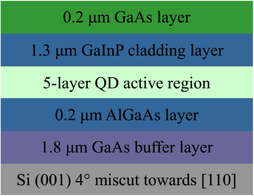
    Fig. 1. Schematic of the test structure of the QD active region on silicon.
    Room-temperature photoluminescence spectra of the samples with Ga0.51In0.49P layer grown at different temperatures.
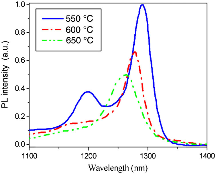
    Fig. 2. Room-temperature photoluminescence spectra of the samples with Ga0.51In0.49P layer grown at different temperatures.
    (a) Schematic of the QD laser structure on Si with the GaInP upper cladding layer. (b) 1 μm×1 μm AFM image of uncapped InAs QDs grown with the same conditions. (c) Cross-sectional TEM image of GaAs grown on Si by the three-step growth method.
    Fig. 3. (a) Schematic of the QD laser structure on Si with the GaInP upper cladding layer. (b) 1  μm×1  μm AFM image of uncapped InAs QDs grown with the same conditions. (c) Cross-sectional TEM image of GaAs grown on Si by the three-step growth method.
    Doping profile of the main laser structure grown on silicon.
    Fig. 4. Doping profile of the main laser structure grown on silicon.
    (a) Schematic of the device structure. (b) Cross-sectional SEM image of the part of a device structure.
    Fig. 5. (a) Schematic of the device structure. (b) Cross-sectional SEM image of the part of a device structure.
    Light–current characteristics of a broad-stripe laser measured under CW condition at room temperature.
    Fig. 6. Light–current characteristics of a broad-stripe laser measured under CW condition at room temperature.
    L-I characteristics of the laser under CW conditions at different operation temperatures.
    Fig. 7. L-I characteristics of the laser under CW conditions at different operation temperatures.
    Jun Wang, Haiyang Hu, Haiying Yin, Yiming Bai, Jian Li, Xin Wei, Yuanyuan Liu, Yongqing Huang, Xiaomin Ren, Huiyun Liu. 1.3  μm InAs/GaAs quantum dot lasers on silicon with GaInP upper cladding layers[J]. Photonics Research, 2018, 6(4): 321
    Download Citation