Contents


2018
Volume: 6 Issue 4
19 Article(s)
Export citation format
NON-HERMITIAN PHOTONICS IN COMPLEX MEDIA: PT-SYMMETRY AND BEYOND
Dispersive non-Hermitian optical heterostructures
O. V. Shramkova, K. G. Makris, D. N. Christodoulides, and G. P. Tsironis
The effect of material dispersion on the optical properties of one-dimensional non-Hermitian scattering systems is investigated in detail. In particular, multilayer heterostructures with gain and loss (parity-time symmetric or not) are examined by taking into account the dispersion of each layer. The exceptional points and phase transitions are characterized based on the spectrum of the corresponding scattering matrix. We demonstrate that an on-average lossy heterostructure can amplify an incident plane wave in the frequency range associated with the emission frequency of the layer with gain.The effect of material dispersion on the optical properties of one-dimensional non-Hermitian scattering systems is investigated in detail. In particular, multilayer heterostructures with gain and loss (parity-time symmetric or not) are examined by taking into account the dispersion of each layer. The exceptional points and phase transitions are characterized based on the spectrum of the corresponding scattering matrix. We demonstrate that an on-average lossy heterostructure can amplify an incident plane wave in the frequency range associated with the emission frequency of the layer with gain..
Photonics Research
- Publication Date: Jan. 30, 2018
- Vol. 6, Issue 4, A1 (2018)


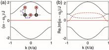
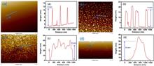
Non-Hermitian lattices with a flat band and polynomial power increase [Invited] | On the Cover
Li Ge
In this work, we first discuss systematically three general approaches to construct a non-Hermitian flat band, defined by its dispersionless real part. These approaches resort to, respectively, spontaneous restoration of non-Hermitian particle-hole symmetry, a persisting flat band from the underlying Hermitian system, and a compact Wannier function that is an eigenstate of the entire system. For the last approach in particular, we show the simplest lattice structure where it can be applied, and we further identify a special case of such a flat band where every point in the Brillouin zone is an exceptional point of order 3. A localized excitation in this “EP3 flat band” can display either a conserved power, quadratic power increase, or even quartic power increase, depending on whether the localized eigenstate or one of the two generalized eigenvectors is initially excited. Nevertheless, the asymptotic wave function in the long time limit is always given by the eigenstate, in this case, the compact Wannier function or its superposition in two or more unit cells.In this work, we first discuss systematically three general approaches to construct a non-Hermitian flat band, defined by its dispersionless real part. These approaches resort to, respectively, spontaneous restoration of non-Hermitian particle-hole symmetry, a persisting flat band from the underlying Hermitian system, and a compact Wannier function that is an eigenstate of the entire system. For the last approach in particular, we show the simplest lattice structure where it can be applied, and we further identify a special case of such a flat band where every point in the Brillouin zone is an exceptional point of order 3. A localized excitation in this “EP3 flat band” can display either a conserved power, quadratic power increase, or even quartic power increase, depending on whether the localized eigenstate or one of the two generalized eigenvectors is initially excited. Nevertheless, the asymptotic wave function in the long time limit is always given by the eigenstate, in this case, the compact Wannier function or its superposition in two or more unit cells..
Photonics Research
- Publication Date: Mar. 05, 2018
- Vol. 6, Issue 4, A10 (2018)

Bistable lasing in parity-time symmetric coupled fiber rings
Sergey V. Smirnov, Maxim O. Makarenko, Sergey V. Suchkov, Dmitry Churkin, and Andrey A. Sukhorukov
We propose a parity-time (PT) symmetric fiber laser composed of two coupled ring cavities with gains and losses, which operates both in PT-symmetric and symmetry-broken regimes depending on the static phase shifts. We perform analytical and numerical analysis by the transfer matrix method taking into account gain saturation and predict laser bistability in the PT-symmetric regime in contrast to a symmetry-broken single-mode operation. In the PT-broken regime, the generation power counterintuitively increases with an increase of the cavity losses.We propose a parity-time (PT) symmetric fiber laser composed of two coupled ring cavities with gains and losses, which operates both in PT-symmetric and symmetry-broken regimes depending on the static phase shifts. We perform analytical and numerical analysis by the transfer matrix method taking into account gain saturation and predict laser bistability in the PT-symmetric regime in contrast to a symmetry-broken single-mode operation. In the PT-broken regime, the generation power counterintuitively increases with an increase of the cavity losses..
Photonics Research
- Publication Date: Mar. 20, 2018
- Vol. 6, Issue 4, A18 (2018)
Photon-pair generation in a quadratically nonlinear parity-time symmetric coupler
Diana A. Antonosyan, Alexander S. Solntsev, and Andrey A. Sukhorukov
Integrated nonlinear waveguide structures enable generation of quantum entangled photons. We describe theoretically the effects of spatially inhomogeneous loss on the creation of photon pairs through spontaneous parametric down-conversion in quadratically nonlinear directional couplers, where photons experience effective parity-time (PT) symmetric potential due to the presence of optical loss in one of the waveguides. We show that for losses below the PT-breaking threshold, the quantum photon states can be flexibly tuned similarly to conservative couplers, whereas for stronger losses, the correlations between two waveguide modes are suppressed. We also formulate a quantum-classical correspondence with sum-frequency generation for fast evaluation of device performance. These results can be applied for the design of quantum plasmonic circuits.Integrated nonlinear waveguide structures enable generation of quantum entangled photons. We describe theoretically the effects of spatially inhomogeneous loss on the creation of photon pairs through spontaneous parametric down-conversion in quadratically nonlinear directional couplers, where photons experience effective parity-time (PT) symmetric potential due to the presence of optical loss in one of the waveguides. We show that for losses below the PT-breaking threshold, the quantum photon states can be flexibly tuned similarly to conservative couplers, whereas for stronger losses, the correlations between two waveguide modes are suppressed. We also formulate a quantum-classical correspondence with sum-frequency generation for fast evaluation of device performance. These results can be applied for the design of quantum plasmonic circuits..
Photonics Research
- Publication Date: Feb. 12, 2018
- Vol. 6, Issue 4, A6 (2018)
Research Articles
Integrated Optics
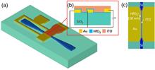
Ultra-compact and broadband electro-absorption modulator using an epsilon-near-zero conductive oxide
Qian Gao, Erwen Li, and Alan X. Wang
Transparent conductive oxides have emerged as a new type of plasmonic material and demonstrated unique electro-optic (E-O) modulation capabilities for next-generation photonic devices. In this paper, we report an ultra-compact, broadband electro-absorption (EA) modulator using an epsilon-near-zero (ENZ) indium-tin oxide (ITO). The device is fabricated on a standard silicon-on-insulator platform through the integration with a 3 μm long, 300 nm wide gold plasmonic slot waveguide. The active E-O modulation region consists of a metal–HfO2–ITO capacitor that can electrically switch the ITO into ENZ with ultra-high modulation strengths of 2.62 and 1.5 dB/μm in simulation and experiment, respectively. The EA modulator also demonstrated a uniform E-O modulation with 70 nm optical bandwidth from 1530 to 1600 nm wavelength.Transparent conductive oxides have emerged as a new type of plasmonic material and demonstrated unique electro-optic (E-O) modulation capabilities for next-generation photonic devices. In this paper, we report an ultra-compact, broadband electro-absorption (EA) modulator using an epsilon-near-zero (ENZ) indium-tin oxide (ITO). The device is fabricated on a standard silicon-on-insulator platform through the integration with a 3 μm long, 300 nm wide gold plasmonic slot waveguide. The active E-O modulation region consists of a metal–HfO 2
Photonics Research
- Publication Date: Mar. 22, 2018
- Vol. 6, Issue 4, 277 (2018)
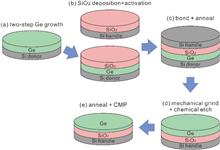
High-performance AlGaInP light-emitting diodes integrated on silicon through a superior quality germanium-on-insulator
Yue Wang, Bing Wang, Wardhana A. Sasangka, Shuyu Bao... and Kwang Hong Lee|Show fewer author(s)
High-performance GaInP/AlGaInP multi-quantum well light-emitting diodes (LEDs) grown on a low threading dislocation density (TDD) germanium-on-insulator (GOI) substrate have been demonstrated. The low TDD of the GOI substrate is realized through Ge epitaxial growth, wafer bonding, and layer transfer processes on 200 mm wafers. With O2 annealing, the TDD of the GOI substrate can be reduced to ~1.2×106 cm 2. LEDs fabricated on this GOI substrate exhibit record-high optical output power of 1.3 mW at a 670 nm peak wavelength under 280 mA current injection. This output power level is at least 2 times higher compared to other reports of similar devices on a silicon (Si) substrate without degrading the electrical performance. These results demonstrate great promise for the monolithic integration of visible-band optical sources with Si-based electronic circuitry and realization of high-density RGB (red, green, and blue) micro-LED arrays with control circuitry.High-performance GaInP/AlGaInP multi-quantum well light-emitting diodes (LEDs) grown on a low threading dislocation density (TDD) germanium-on-insulator (GOI) substrate have been demonstrated. The low TDD of the GOI substrate is realized through Ge epitaxial growth, wafer bonding, and layer transfer processes on 200 mm wafers. With O 2 ~ 1.2 × 10 6 cm 2
Photonics Research
- Publication Date: Mar. 28, 2018
- Vol. 6, Issue 4, 290 (2018)
Lasers and Laser Optics
High-quality 2-μm Q-switched pulsed solid-state lasers using spin-coating-coreduction approach synthesized Bi2Te3 topological insulators
Junpeng Qiao, Shengzhi Zhao, Kejian Yang, Wei-Heng Song... and Chao-Kuei Lee|Show fewer author(s)
In this paper, the fabrication process and characterization of Bi2Te3 topological insulators (TIs) synthesized by the spin-coating-coreduction approach (SCCA) is reported. With this approach, high-uniformity nano-crystalline show moreIn this paper, the fabrication process and characterization of Bi 2 Te 3 Q Q
Photonics Research
- Publication Date: Mar. 27, 2018
- Vol. 6, Issue 4, 314 (2018)
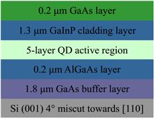
1.3 μm InAs/GaAs quantum dot lasers on silicon with GaInP upper cladding layers
Jun Wang, Haiyang Hu, Haiying Yin, Yiming Bai... and Huiyun Liu|Show fewer author(s)
We report on the first electrically pumped continuous-wave (CW) InAs/GaAs quantum dot (QD) laser grown on Si with a GaInP upper cladding layer. A QD laser structure with a Ga0.51In0.49P upper cladding layer and an Al0.53Ga0.47As lower cladding layer was directly grown on Si by metal–organic chemical vapor deposition. It demonstrates the postgrowth annealing effect on the QDs was relieved enough with the GaInP upper cladding layer grown at a low temperature of 550°C. Broad-stripe edge-emitting lasers with 2-mm cavity length and 15-μm stripe width were fabricated and characterized. Under CW operation, room-temperature lasing at ~1.3 μm has been achieved with a threshold density of 737 A/cm2 and a single-facet output power of 21.8 mW.We report on the first electrically pumped continuous-wave (CW) InAs/GaAs quantum dot (QD) laser grown on Si with a GaInP upper cladding layer. A QD laser structure with a Ga 0.51 In 0.49 P Al 0.53 Ga 0.47 As ~ 1.3 μm 737 A / cm 2
Photonics Research
- Publication Date: Mar. 27, 2018
- Vol. 6, Issue 4, 321 (2018)
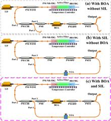
Noise-sidebands-free and ultra-low-RIN 1.5 μm single-frequency fiber laser towards coherent optical detection
Qilai Zhao, Zhitao Zhang, Bo Wu, Tianyi Tan... and Shanhui Xu|Show fewer author(s)
A noise-sidebands-free and ultra-low relative intensity noise (RIN) 1.5 μm single-frequency fiber laser is demonstrated for the first time to our best knowledge. Utilizing a self-injection locking framework and a booster optical amplifier, the noise sidebands with relative amplitudes as high as 20 dB are completely suppressed. The RIN is remarkably reduced by more than 64 dB at the relaxation oscillation peak to retain below 150 dB/Hz in a frequency range from 75 kHz to 50 MHz, while the quantum noise limit is 152.9 dB/Hz. Furthermore, a laser linewidth narrower than 600 Hz, a polarization-extinction ratio of more than 23 dB, and an optical signal-to-noise ratio of more than 73 dB are acquired simultaneously. This noise-sidebands-free and ultra-low-RIN single-frequency fiber laser is highly competitive in advanced coherent light detection fields including coherent Doppler wind lidar, high-speed coherent optical communication, and precise absolute distance coherent measurement.A noise-sidebands-free and ultra-low relative intensity noise (RIN) 1.5 μm single-frequency fiber laser is demonstrated for the first time to our best knowledge. Utilizing a self-injection locking framework and a booster optical amplifier, the noise sidebands with relative amplitudes as high as 20 dB are completely suppressed. The RIN is remarkably reduced by more than 64 dB at the relaxation oscillation peak to retain below 150 dB / Hz 152.9 dB / Hz
Photonics Research
- Publication Date: Mar. 27, 2018
- Vol. 6, Issue 4, 326 (2018)

Evanescent-wave pumped single-mode microcavity laser from fiber of 125 μm diameter
Yuchen Wang, Shu Hu, Xiao Yang, Ruizhi Wang... and Chuanxiang Sheng|Show fewer author(s)
A microcavity laser based on evanescent-wave-coupled gain is formed using a silica fiber with a diameter of 125 μm in a rhodamine 6G ethanol solution. When the fiber is sticking to the cuvette wall by capillary force, using the excitation of a 532 nm nanosecond pulsed laser, single-mode laser emission is observed. While increasing the distance between the fiber and the cuvette wall, the typical multi-peak whispering-gallery-mode (WGM) laser emission can also be demonstrated. On the other hand, while increasing the refractive index of the solution by mixing ethanol and ethylene glycol with different ratios as a solvent, the single-mode emission would evolve to multi-peak WGM laser emission controllably.A microcavity laser based on evanescent-wave-coupled gain is formed using a silica fiber with a diameter of 125 μm in a rhodamine 6G ethanol solution. When the fiber is sticking to the cuvette wall by capillary force, using the excitation of a 532 nm nanosecond pulsed laser, single-mode laser emission is observed. While increasing the distance between the fiber and the cuvette wall, the typical multi-peak whispering-gallery-mode (WGM) laser emission can also be demonstrated. On the other hand, while increasing the refractive index of the solution by mixing ethanol and ethylene glycol with different ratios as a solvent, the single-mode emission would evolve to multi-peak WGM laser emission controllably..
Photonics Research
- Publication Date: Mar. 27, 2018
- Vol. 6, Issue 4, 332 (2018)
Materials
Broadening and enhancing 2.7 μm emission spectra in Er/Ho co-doped oxyfluoride germanosilicate glass ceramics by imparting multiple local structures to rare earth ions
Qunhuo Liu, Ying Tian, Wenhua Tang, Feifei Huang... and Shiqing Xu|Show fewer author(s)
Er/Ho co-doped oxyfluoride germanosilicate glass and glass ceramics are prepared and compared. The results indicate that the glass consists of SiO4 and GeO4 structural units, while the network of the glass ceramics consists of SiO4, GeO4, and GeO6 units together with NaYF4 nanocrystals. The presence of multiple local structures in glass ceramics creates a range of dipole environments, which is beneficial to the broadening of 2.7 μm emission. Two other reasons are attributed to the broadening of 2.7 μm emission in glass ceramics: the energy-level splitting of Er3+ and the enhancement of the Ho3+:I65→I75 transition in NaYF4 nanocrystals.Er/Ho co-doped oxyfluoride germanosilicate glass and glass ceramics are prepared and compared. The results indicate that the glass consists of SiO 4 GeO 4 SiO 4 GeO 4 GeO 6 NaYF 4 Er 3 + Ho 3 + : I 6 5 → I 7 5 NaYF 4
Photonics Research
- Publication Date: Mar. 29, 2018
- Vol. 6, Issue 4, 339 (2018)
Nanomaterials
Graphitic carbon nitride, a saturable absorber material for the visible waveband
Mengxia Wang, Fukun Ma, Zhengping Wang, Dawei Hu... and Xiaopeng Hao|Show fewer author(s)
For the first time to our knowledge, graphitic carbon nitride (g-C3N4) nanosheets are found to be an excellent saturable absorber material in the visible waveband. g-C3N4 exhibits much stronger saturable absorption in this region than in the near-infrared region, unlike other two-dimensional materials such as graphene and black phosphorus. By the Z-scan method, the nonlinear absorption coefficient β of the material is first measured at three visible wavelengths, and for g-C3N4 it is 2.05, 0.34, and 0.11 cm·GW 1 at 355, 532, and 650 nm, respectively. These are much larger than 0.06 cm·GW 1 at 1064 nm.For the first time to our knowledge, graphitic carbon nitride (g - C 3 N 4 g - C 3 N 4 β g - C 3 N 4 2.05 0.34 0.11 cm · GW 1 0.06 cm · GW 1
Photonics Research
- Publication Date: Mar. 27, 2018
- Vol. 6, Issue 4, 307 (2018)
Nonlinear Optics
Influences of multiphoton absorption and free-carrier effects on frequency-comb generation in normal dispersion silicon microresonators
Mulong Liu, Leiran Wang, Qibing Sun, Siqi Li... and Wei Zhao|Show fewer author(s)
We investigate frequency-comb generation in normal dispersion silicon microresonators from the near-infrared to mid-infrared wavelength range in the presence of multiphoton absorption and free-carrier effects. It is found thashow moreWe investigate frequency-comb generation in normal dispersion silicon microresonators from the near-infrared to mid-infrared wavelength range in the presence of multiphoton absorption and free-carrier effects. It is found that parametric oscillation is inhibited in the telecom wavelength range resulting from strong two-photon absorption. On the contrary, beyond the wavelength of 2200 nm, where three- and four-photon absorption are less detrimental, a comb can be generated with moderate pump power, or free-carriers are swept out by a positive-intrinsic-negative structure. In the temporal domain, the generated combs correspond to flat-top pulses, and the pulse duration can be easily controlled by varying the laser detuning. The reported comb generation process shows a high conversion efficiency compared with anomalous dispersion regime, which can guide and promote comb formation in materials with normal dispersion. As the comb spectra cover the mid-infrared wavelength range, they can find applications in comb-based radiofrequency photonic filters and mid-infrared spectroscopy..
Photonics Research
- Publication Date: Mar. 19, 2018
- Vol. 6, Issue 4, 238 (2018)
Optical Materials
Emerging photoluminescence from defective vanadium diselenide nanosheets
Amir Ghobadi, Turkan Gamze Ulusoy Ghobadi, Ali Kemal Okyay, and Ekmel Ozbay
In this paper, for the first time to our knowledge in the literature, we demonstrate photoluminescence from two-dimensional (2D) vanadium diselenide (VSe2) nanosheets (NSs). The preparation of these nanostructures is carried out with a combinational method based on nanosecond pulsed laser ablation (PLA) and chemical exfoliation. For this aim, VSe2 bulk is first ablated into nanoparticles (NPs) inside a water solution. Afterward, NPs are chemically exfoliated into NSs using lithium intercalation via ultrasonic treatment. Although VSe2 is a semimetal in its bulk form, its nanostructures show photo-responsive behavior, and it turns into a strongly luminescent material when it is separated into NSs. Based on the obtained results, the surface defects induced during the PLA process are the origin of this photoluminescence from NSs. Our findings illustrate that this new material can be a promising semiconductor for photovoltaic and light emitting diode applications.In this paper, for the first time to our knowledge in the literature, we demonstrate photoluminescence from two-dimensional (2D) vanadium diselenide (VSe 2 VSe 2 VSe 2
Photonics Research
- Publication Date: Mar. 22, 2018
- Vol. 6, Issue 4, 244 (2018)
Photonic Crystals and Devices
Enhanced complete photonic bandgap in a moderate refractive index contrast chalcogenide-air system with connected-annular-rods photonic crystals
Jin Hou, Chunyong Yang, Xiaohang Li, Zhenzhou Cao, and Shaoping Chen
Connected-annular-rods photonic crystals (CARPCs) in both triangular and square lattices are proposed to enhance the two-dimensional complete photonic bandgap (CPBG) for chalcogenide material systems with moderate refractive index contrast. For the typical chalcogenide-glass–air system with an index contrast of 2.8:1, the optimized square lattice CARPC exhibits a significantly larger normalized CPBG of about 13.50%, though the use of triangular lattice CARPC is unable to enhance the CPBG. It is almost twice as large as our previously reported result [IEEE J. Sel. Top. Quantum Electron.22, 4900108 (2016)IJSQEN1077-260X10.1109/JSTQE.2015.2422997]. Moreover, the CPBG of the square-lattice CARPC could remain until an index contrast as low as 2.24:1. The result not only favors wideband CPBG applications for index contrast systems near 2.8:1, but also makes various optical applications that are dependent on CPBG possible for more widely refractive index contrast systems.Connected-annular-rods photonic crystals (CARPCs) in both triangular and square lattices are proposed to enhance the two-dimensional complete photonic bandgap (CPBG) for chalcogenide material systems with moderate refractive index contrast. For the typical chalcogenide-glass–air system with an index contrast of 2.8:1, the optimized square lattice CARPC exhibits a significantly larger normalized CPBG of about 13.50%, though the use of triangular lattice CARPC is unable to enhance the CPBG. It is almost twice as large as our previously reported result [IEEE J. Sel. Top. Quantum Electron.22 , 4900108 (2016 )IJSQEN 1077-260X 10.1109/JSTQE.2015.2422997
Photonics Research
- Publication Date: Mar. 28, 2018
- Vol. 6, Issue 4, 282 (2018)
Polarization
Highly efficient generation of arbitrary vector beams with tunable polarization, phase, and amplitude
Sheng Liu, Shuxia Qi, Yi Zhang, Peng Li... and Jianlin Zhao|Show fewer author(s)
We propose an efficient and robust method to generate tunable vector beams by employing a single phase-type spatial light modulator (SLM). With this method, a linearly polarized Gaussian beam can be converted into a vector beam with arbitrarily controllable polarization state, phase, and amplitude. The energy loss during the conversion is greatly reduced and depends mainly on the reflectivity of the SLM. We experimentally demonstrate that conversion efficiency of about 47% is achieved by using an SLM with reflectivity of 62%. Several typical vector beams, including cylindrical vector beams, vector beams on higher order Poincaré spheres, and arbitrary vector beams attached with phases and with tunable amplitude, are generated and verified experimentally. This method is also expected to create high-power vector beams and play important roles in optical fabrication and light trapping.We propose an efficient and robust method to generate tunable vector beams by employing a single phase-type spatial light modulator (SLM). With this method, a linearly polarized Gaussian beam can be converted into a vector beam with arbitrarily controllable polarization state, phase, and amplitude. The energy loss during the conversion is greatly reduced and depends mainly on the reflectivity of the SLM. We experimentally demonstrate that conversion efficiency of about 47% is achieved by using an SLM with reflectivity of 62%. Several typical vector beams, including cylindrical vector beams, vector beams on higher order Poincaré spheres, and arbitrary vector beams attached with phases and with tunable amplitude, are generated and verified experimentally. This method is also expected to create high-power vector beams and play important roles in optical fabrication and light trapping..
Photonics Research
- Publication Date: Mar. 01, 2018
- Vol. 6, Issue 4, 228 (2018)
Silicon Photonics
Mid-infrared silicon photonic waveguides and devices [Invited]
Yi Zou, Swapnajit Chakravarty, Chi-Jui Chung, Xiaochuan Xu, and Ray T. Chen
Silicon has been the material of choice of the photonics industry over the last decade due to its easy integration with silicon electronics, high index contrast, small footprint, and low cost, as well as its optical transpareshow moreSilicon has been the material of choice of the photonics industry over the last decade due to its easy integration with silicon electronics, high index contrast, small footprint, and low cost, as well as its optical transparency in the near-infrared and parts of mid-infrared (MIR) wavelengths (from 1.1 to 8 μm). While considerations of micro- and nano-fabrication-induced device parameter deviations and a higher-than-desirable propagation loss still serve as a bottleneck in many on-chip data communication applications, applications as sensors do not require similar stringent controls. Photonic devices on chips are increasingly being demonstrated for chemical and biological sensing with performance metrics rivaling benchtop instruments and thus promising the potential of portable, handheld, and wearable monitoring of various chemical and biological analytes. In this paper, we review recent advances in MIR silicon photonics research. We discuss the pros and cons of various platforms, the fabrication procedures for building such platforms, and the benchmarks demonstrated so far, together with their applications. Novel device architectures and improved fabrication techniques have paved a viable way for realizing low-cost, high-density, multi-function integrated devices in the MIR. These advances are expected to benefit several application domains in the years to come, including communication networks, sensing, and nonlinear systems..
Photonics Research
- Publication Date: Mar. 22, 2018
- Vol. 6, Issue 4, 254 (2018)
Spectroscopy
X-ray absorption spectroscopy study of energy transport in foil targets heated by petawatt laser pulses
I. Y. Skobelev, S. N. Ryazantsev, D. D. Arich, P. S. Bratchenko... and S. A. Pikuz|Show fewer author(s)
X-ray absorption spectroscopy is proposed as a method for studying the heating of solid-density matter excited by secondary X-ray radiation from a relativistic laser-produced plasma. The method was developed and applied to experiments involving thin silicon foils irradiated by 0.5–1.5 ps duration ultrahigh contrast laser pulses at intensities between 0.5×10²⁰ and 2.5×10²⁰ W/cm2. The electron temperature of the material at the rear side of the target is estimated to be in the range of 140–300 eV. The diagnostic approach enables the study of warm dense matter states with low self-emissivity.X-ray absorption spectroscopy is proposed as a method for studying the heating of solid-density matter excited by secondary X-ray radiation from a relativistic laser-produced plasma. The method was developed and applied to experiments involving thin silicon foils irradiated by 0.5–1.5 ps duration ultrahigh contrast laser pulses at intensities between 0.5 × 10 20 2.5 × 10 20 W / cm 2
Photonics Research
- Publication Date: Mar. 02, 2018
- Vol. 6, Issue 4, 234 (2018)
Ultrafast Optics
Clue to a thorough understanding of terahertz pulse generation by femtosecond laser filamentation
Jiayu Zhao, Weiwei Liu, Shichang Li, Dan Lu... and Songlin Zhuang|Show fewer author(s)
In this work, it has been demonstrated that in order to fully understand the terahertz (THz) pulse generation process during femtosecond laser filamentation, the interaction between THz wave and air plasma has to be taken into account. This interaction is mainly associated with the spatial confinement of the THz pulse by the plasma column, which could be described by the one-dimensional negative dielectric (1DND) waveguide model. By combining the 1DND model with the conventional four-wave mixing (4WM) and photocurrent (PC) models, the variation of THz spectral amplitude and width obtained in experiments could be better understood. Finally, a three-step procedure, with 1DND bridging 4WM and PC processes, has been established for the first time to describe the underlying mechanism of THz radiation from plasma sources.In this work, it has been demonstrated that in order to fully understand the terahertz (THz) pulse generation process during femtosecond laser filamentation, the interaction between THz wave and air plasma has to be taken into account. This interaction is mainly associated with the spatial confinement of the THz pulse by the plasma column, which could be described by the one-dimensional negative dielectric (1DND) waveguide model. By combining the 1DND model with the conventional four-wave mixing (4WM) and photocurrent (PC) models, the variation of THz spectral amplitude and width obtained in experiments could be better understood. Finally, a three-step procedure, with 1DND bridging 4WM and PC processes, has been established for the first time to describe the underlying mechanism of THz radiation from plasma sources..
Photonics Research
- Publication Date: Mar. 27, 2018
- Vol. 6, Issue 4, 296 (2018)
About the Cover
Temporal disparity and intensity fluctuation of photon pulses in a polarization-based QKD system with and without side channel effects.

© Copyright 2018-2021 | Chinese Laser Press. All Rights Reserved 沪ICP备15018463号-20