Author Affiliations
1State Key Laboratory of Information Photonics and Optical Communications, Beijing University of Posts and Telecommunications, Beijing 100876, China2State Key Laboratory of Alternate Electrical Power System with Renewable Energy Sources, North China Electric Power University, Beijing 102206, China3Laboratory of Nano Optoelectronics, Institute of Semiconductors, Chinese Academy of Sciences, Beijing 100083, China4Engineering Research Center for Semiconductor Integrated Technology, Institute of Semiconductors, Chinese Academy of Sciences, Beijing 100083, China5Department of Electronic & Electrical Engineering, University College London, London WC1E 7JE, UKshow less
Abstract
We report on the first electrically pumped continuous-wave (CW) InAs/GaAs quantum dot (QD) laser grown on Si with a GaInP upper cladding layer. A QD laser structure with a upper cladding layer and an lower cladding layer was directly grown on Si by metal–organic chemical vapor deposition. It demonstrates the postgrowth annealing effect on the QDs was relieved enough with the GaInP upper cladding layer grown at a low temperature of 550°C. Broad-stripe edge-emitting lasers with 2-mm cavity length and 15-μm stripe width were fabricated and characterized. Under CW operation, room-temperature lasing at has been achieved with a threshold density of and a single-facet output power of 21.8 mW.1. INTRODUCTION
Driven by on-chip optical interconnects instead of electrical links, silicon photonics has attracted increasing attention due to its potential prospects in applications [1–3]. Much effort has been made to realize laser sources on an Si platform, such as Si Raman lasers [4], Si hybrid lasers [5], GeSi lasers on Si [6], and GeSn lasers on Si [7]. Among these efforts, the integration of III-V lasers monolithically grown on Si is considered to be a promising solution to obtain efficient light sources on the Si platform in the near future [8–11]. However, direct epitaxial growth of III-V semiconductors on Si wafers faces several significant difficulties including large mismatches in lattice constant, thermal expansion coefficient, and polar/nonpolar surfaces [12,13]. These issues induce the formation of different types of defects, thermal cracks, and antiphase boundaries [14,15].
Due to the tolerance to the crystalline defects, quantum dot (QD) lasers have shown promise for fabricating high performance lasers on Si. To date, III-V QD lasers directly grown on Si have made great progress in recent years [10,16–19]. Several research groups studying 1.3 μm InAs/GaAs QD lasers monolithically grown on Si have demonstrated impressive results. In 2011, a laser structure grown on silicon was realized with a QD active region and 1.5-μm - and cladding layers. A threshold current density of was achieved under pulsed operation at room temperature [16]. Then, continuous-wave (CW) operation was achieved with a threshold current density of at room temperature [10]. In 2014, a threshold current density of () was demonstrated under CW operation at room temperature. Its structure on Ge/Si substrates includes an InAs QD active region and 1.4-μm - and cladding layers [17]. After that, a laser on GaP/Si substrates was achieved with a high wall-plug efficiency of 38.4% under CW operation at room temperature [18]. In 2016, a room-temperature microdisk laser with a QD active region grown on Si was realized, and the lasing threshold is similar to that on GaAs substrates [19].
It is worth noting that the AlGaAs layers as both bottom and upper cladding layers were adopted in the QD laser structures on Si and were grown by molecular beam epitaxy (MBE) technology in the reports mentioned previously [16–19]. To our knowledge, QD laser structures grown on silicon by only metal–organic chemical vapor deposition (MOCVD) have not been reported up to now. The main reason involves problems with the growth of the AlGaAs upper cladding layer by MOCVD [20,21].
Sign up for Photonics Research TOC. Get the latest issue of Photonics Research delivered right to you!Sign up now
For the growth of AlGaAs upper cladding layers, a high growth temperature (generally above 700°C) is required to obtain high quality in both electric and optical properties. However, for the QD active region, at a high temperature, the degradation of the optical quality, such as blueshift of emission wavelength and reduction of optical gain, should occur after growth of AlGaAs upper cladding layers [22,23].
Actually, it is important to develop strategies to grow QD laser structures on Si by MOCVD technology. There are three main advantages for MOCVD-based fabrications: (1) high growth rates and low costs in volume production requirements; (2) regrowth or selective area growth required by distributed feedback lasers and optical integrated structures and devices; and (3) high-temperature in situ annealing for GaAs/Si buffer layer growth processes [20,24].
To avoid the growth condition conflict between QD active regions and AlGaAs upper cladding layers, it is a reasonable solution to adopt the GaInP upper cladding layers instead. Compared with AlGaAs upper cladding layers, the GaInP counterparts have two main advantages. One, their growth temperature by MOCVD can be lowered to 500°C. Hence, it can be relieved to affect the QDs during postgrowth of upper cladding layers. The other advantage is that GaInP is a kind of Al-free semiconductor material and is relatively insensitive to impurities, such as oxygen and carbon, during material growth processes [25].
In this paper, the purpose is to develop a 1.3 μm InAs/GaAs QD laser structure grown on silicon by MOCVD technology with a GaInP upper cladding layer and AlGaAs lower cladding layer. The postgrowth annealing effect on the QDs was relieved enough through the GaInP upper cladding layer with a low growth temperature. The broad-stripe edge-emitting lasers with 2-mm cavity length and 15-μm stripe width were fabricated and characterized. The device lasing at with threshold density of and single-facet output power of 21.8 mW was achieved under CW condition at room temperature.
2. OPTIMIZATION OF GROWTH CONDITIONS OF GaInP UPPER CLADDING LAYER
To study the influence of the postgrowth process of the upper cladding layer over the QDs, a test structure of 1.3 μm InAs/GaAs QD lasers directly grown on silicon, as shown in Fig. 1, was grown to explore the optical properties of the QDs after the growth process of the upper GaInP cladding layers at different growth temperatures. The test structure begins with a 1.8-μm GaAs buffer layer, followed by an active region with five-layer InAs/InGaAs/GaAs QDs surrounded by a 0.2-μm layer and a 1.3-μm layer. Finally, it is capped with a 0.2-μm GaAs layer.
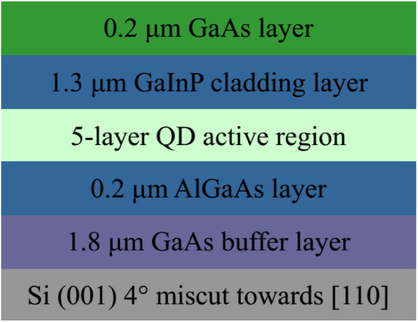
Figure 1.Schematic of the test structure of the QD active region on silicon.
The growth of the test structure on Si was carried out on the Aixtron-200 MOCVD system. High-purity trimethylgallium (TMGa), trimethylindium (TMIn), trimethylaluminum (TMAl), arsine (), phosphine (), silane (), and diethylzinc (DEZn) were used as source materials. The carrier gas was Pd-cell purified hydrogen. The 2-in. (5.08 cm) (100)-oriented Si wafers misoriented 4° toward the [011] direction were used as the substrates. The growth temperature was measured by a thermocouple under the graphite susceptor in the reactor chamber. After chemical cleaning, the surface of the Si wafer was hydrogenated by dipping in the diluted HF solution. Immediately, the Si wafers were loaded into the reactor chamber of the MOCVD system and baked at 220°C for 30 min. Then the wafers were arsenic passivated at 750°C for 15 min in arsine and hydrogen ambient. Next, the three-step growth process was performed to deposit the GaAs buffer layer. The temperature was first decreased to 420°C for growth of a low-temperature GaAs nucleation layer with thickness of 15 nm. Then a moderate-temperature GaAs layer with thickness of 300 nm was grown on the nucleation layer at 630°C. After increasing temperature, a high-temperature GaAs layer with thickness of 1500 nm was grown at 680°C with insertions of two sets of thermal cycle annealing (TCA) process at different positions. The process employed here was previously optimized, and the details of the growth process were presented in our previous works [15,26]. For the three-step growth, the thickness of the whole GaAs buffer layer was 1.8 μm.
After the three-step growth and TCA process, a 200-nm layer was grown when the temperature was increased to 720°C. Then, as the temperature was decreased to 600°C, the five-layer InAs/InGaAs/GaAs QD structure started to grow, and each QD layer structure included a 2-nm layer, a 2.6-ML (monolayer) InAs QD layer, a 6-nm layer, a 5-nm GaAs layer, and a 50-nm GaAs spacer layer. For QD layers, the growth temperate and growth rate were 480°C and 0.036 ML/s, and the V/III ratio was 6. The growth temperate for the GaAs spacer layer was 600°C, and for layers was 480°C. The details of the growth processes were similar to our previous works [27,28]. Then, a 1.3-μm layer was grown at three temperatures of 550, 600, and 650°C for each sample with growth rate of 1.0 nm/s. All the epilayers were unintentionally doped.
Figure 2 shows the room-temperature photoluminescence (PL) spectra of the grown samples of the layer at different temperatures. The PL spectra of the samples exhibit an obvious blueshift for higher growth temperatures of the layer. The peak wavelength is 1290, 1278, and 1264 nm for the samples with the layer grown at 550, 600, and 650°C, respectively, and the PL full-width at half-maximum (FWHM) is 41, 43, and 63 nm, respectively. The intensity weakens and the FWHM increases as the growth temperature becomes higher. These results indicate that the postgrowth annealing effect during the upper cladding layer growth can be alleviated and tolerated for an emission wavelength of 1.3 μm when the growth temperature of the upper cladding layer is at 550°C. We believe that there are two main reasons for relieving the postgrowth annealing effect. One involves the relatively low growth temperature (550°C) of the GaInP cladding layer. The other, the relatively thin (1.3 μm) cladding layer and high growth rate (10 Å/s) of GaInP, shorten the postgrowth time to less than 30 min.

Figure 2.Room-temperature photoluminescence spectra of the samples with layer grown at different temperatures.
3. LASER EPITAXIAL STRUCTURE GROWTH AND DEVICE FABRICATION
The whole structure for 1.3 μm InAs/GaAs QD lasers on silicon is shown in Fig. 3(a). After the three-step growth and TCA process of the 1.8-μm GaAs buffer layer, increasing temperature to 720°C, a heavily -type doped 0.5-μm-thick GaAs layer was grown for the ohmic contact. Then, the laser structure was grown mainly consisting of a five-layer InAs/InGaAs/GaAs QD active region surrounded by a 100 nm GaAs waveguide layer, and a 1.3-μm lower cladding layer and a 1.3-μm -GaInP upper cladding layer with doped concentration of about . Finally, a 200-nm -GaAs layer with doped concentration of about was grown as the -side contact layer. and GaInP cladding layers have the same refractive index at the wavelength of 1.3 μm and form a symmetric waveguide structure. The growth temperatures of cladding layer and -GaInP cladding layer were 720 and 550°C, respectively, and and DEZn were the -dopant and -dopant used in the growth. The growth conditions of the QD active region were similar to those of the test structure. The 20-nm AlGaAs layer above the active region was inserted to form a graded energy band and grown at 600°C. Because the growth time of the layer is very short, it almost has no influence on the QD optical properties.
Figure 3.(a) Schematic of the QD laser structure on Si with the GaInP upper cladding layer. (b) AFM image of uncapped InAs QDs grown with the same conditions. (c) Cross-sectional TEM image of GaAs grown on Si by the three-step growth method.
The atomic force microscopy (AFM) image of the uncapped QDs grown with the same conditions is shown in Fig. 3(b). The QDs exhibit good morphology and are almost free of coalescence. Figure 3(c) shows the cross-sectional transmission electron microscopy (TEM) image around the GaAs/Si intersurface. Most of defects are strongly confined in the bottom region of the GaAs buffer layer. The dislocation density of the buffer layer surface is about .
After growth, the doping profile of the main laser structure measured by a capacitance-voltage profiler is shown in Fig. 4. The sample was mounted with front-contact mode, and 0.1 mol/L diaminoethane: ethylenediamine tetraacetic acid was used as the electrolytes for GaInP, GaAs, and AlGaAs. It is indicated that a desired doping profile with a good control for the optical loss and -type contact is achieved.
Figure 4.Doping profile of the main laser structure grown on silicon.
A schematic of the chip structure of the edge-emitting broad-stripe lasers is shown in Fig. 5(a). The stripe width and cavity length are 15 μm and 2 mm for a single chip. For comparison, the cross-sectional scanning electron microscope (SEM) image of a device structure is also shown in Fig. 5(b). The detailed fabrication processes are similar to our previous report [15].
Figure 5.(a) Schematic of the device structure. (b) Cross-sectional SEM image of the part of a device structure.
4. RESULTS AND DISCUSSION
Figure 6 shows light–current (L-I) characteristics of a broad-stripe laser, measured under CW condition at room temperature. The room-temperature threshold current of the laser is 221 mA, corresponding to a threshold current density of . A maximum single-facet output power of 21.8 mW is obtained at the injection current of 1000 mA due to the limit of the current source. The inset of Fig. 6 shows the lasing emission spectrum of the laser operating at two times the threshold current under CW condition. The emission wavelength is 1296.1 nm with a linewidth (FWHM) of 3.1 nm.
Figure 6.Light–current characteristics of a broad-stripe laser measured under CW condition at room temperature.
To further study high-temperature operation characteristics of the laser, its performance at different operation temperatures is shown in Fig. 7. The threshold current increases and the output power decreases rapidly as the operation temperature increases from 20 to 60°C. At the temperature of 60°C, there is an obvious thermal rollover in the L-I curve. The characteristic temperature of the device between 20 and 60°C, as extracted by fitting the threshold current as an exponential function of temperature, is 39 K. For the operation temperature higher than 60°C, the device fails to lase.
Figure 7.L-I characteristics of the laser under CW conditions at different operation temperatures.
The relatively poor characteristic temperature presented here is mainly related to two aspects. One is the still high dislocation density in the active region compared with that of the same laser structure grown on the native GaAs substrates. These dislocations result in nonradiative recombination in the active region and release a large amount of heat energy. The other, the laser structure and growth conditions, especially for the QD active region, need to be further optimized. For the former, an effective dislocation filter structure, such as strained layer superlattices [29] and aspect ratio trapping methods [30], can be applied to reduce the dislocation density of the laser structure during the three-step growth process. Hence, less nonradiative recombination and higher material gain should be expected. For the latter, a modulation -doping of the QD active region could also be adopted to improve the temperature sensitivity of laser devices [31,32]. For the state-of-the-art work of InAs/GaAs QD lasers grown on offcut Si (001) substrates by MBE [10], the threshold current density and maximum single-facet output power are and 52.5 mW, and the CW operation temperature is higher than 75°C. Hence, the laser performance in the present work has a much higher threshold current density, a lower maximum output power, and a poorer characteristic temperature. We believe that better results can be expected with further optimization on the wafer growth using MOCVD technology.
5. CONCLUSION
In conclusion, we have demonstrated the first 1.3 μm InAs/GaAs QD laser directly grown on silicon with a GaInP upper cladding layer. The postgrowth annealing effect on the QDs was relieved enough with the upper cladding layer grown at a low temperature. The broad-stripe edge-emitting lasers with 2-mm cavity length and 15-μm stripe width were fabricated and characterized. The devices exhibited CW lasing at with threshold density of and single-facet output power of 21.8 mW at room temperature. Moreover, these results provide a practical strategy to grow 1.3 μm QD lasers directly on Si only by MOCVD technology. More importantly, with further progress in growth processes on silicon, these Si-based QD lasers with higher performance could be achieved by MOCVD technology, which will significantly promote the commercial development of laser sources in silicon photonics.
References
[1] A. Rickman. The commercialization of silicon photonics. Nat. Photonics, 8, 579-582(2014).
[2] M. Asghari, A. V. Krishnamoorthy. Silicon photonics: energy-efficient communication. Nat. Photonics, 5, 268-270(2011).
[3] Z. Wang, B. Tian, M. Pantouvaki, W. Guo, P. Absil, J. Campenhout, C. Merckling, D. Thourhout. Room-temperature InP distributed feedback laser array directly grown on silicon. Nat. Photonics, 9, 837-842(2015).
[4] S. G. Cloutier, P. A. Kossyrev, J. M. Xu. Optical gain and stimulated emission in periodic nanopatterned crystalline silicon. Nat. Mater., 4, 887-891(2005).
[5] A. W. Fang, H. Park, O. Cohen, R. Jones, M. J. Panicia, J. E. Bowers. Electrically pumped hybrid AlGaInAs-silicon evanescent laser. Opt. Express, 14, 9203-9210(2006).
[6] R. E. Camacho-Aguilera, Y. Cai, N. Patel, J. T. Bessette, M. Romagnoli, L. C. Kimerling, J. Michel. An electrically pumped germanium laser. Opt. Express, 20, 11316-11320(2012).
[7] D. Stange, S. Wirths, R. Geiger, C. Schulte-Braucks, B. Marzban, N. von den Driesch, G. Mussler, T. Zabel, T. Stoica, J.-M. Hartmann, S. Mantl, Z. Ikonic, D. Grützmacher, H. Sigg, J. Witzens, D. Buca. Optically pumped GeSn microdisk lasers on Si. ACS Photon., 3, 1279-1285(2016).
[8] Z. Zhou, B. Yin, J. Michel. On-chip light sources for silicon photonics. Light Sci. Appl., 4, e358(2015).
[9] E. Tournié, L. Cerutti, J. B. Rodriguez, H. Liu, J. Wu, S. Chen. Metamorphic III-V semiconductor lasers grown on silicon. MRS Bull., 41, 218-223(2016).
[10] S. Chen, W. Li, J. Wu, Q. Jiang, M. Tang, S. Shutts, S. N. Elliott, A. Sobiesierski, A. J. Seeds, I. Ross, P. M. Smowton, H. Liu. Electrically pumped continuous-wave III-V quantum dot lasers on silicon. Nat. Photonics, 10, 307-311(2016).
[11] Y. Wan, J. Norman, Q. Li, M. J. Kennedy, D. Liang, C. Zhang, D. Huang, Z. Zhang, A. Y. Liu, A. Torres, D. Jung, A. C. Gossard, E. L. Hu, K. M. Lau. 1.3 μm submilliamp threshold quantum dot micro-lasers on Si. Optica, 4, 940-944(2017).
[12] D. Liang, J. E. Bowers. Recent progress in lasers on silicon. Nat. Photonics, 4, 511-517(2010).
[13] R. Chen, T. T. D. Tran, K. W. Ng, W. S. Ko, L. C. Chuang, F. G. Sedgwick, C. Chang-Hasnain. Nanolasers grown on silicon. Nat. Photonics, 5, 170-175(2011).
[14] A. Y. Liu, R. W. Herrick, O. Ueda, P. M. Petroff, A. C. Gossard, J. E. Bowers. Reliability of InAs/GaAs quantum dot lasers epitaxially grown on silicon. IEEE J. Sel. Top. Quantum Electron., 21, 1900708(2015).
[15] J. Wang, X. Ren, C. Deng, H. Hu, Y. He, Z. Cheng, H. Ma, Q. Wang, Y. Huang, X. Duan, X. Yan. Extremely low-threshold current density InGaAs/AlGaAs quantum-well lasers on silicon. J. Lightwave Technol., 33, 3163-3169(2015).
[16] T. Wang, H. Liu, A. Lee, F. Pozzi, A. Seeds. 1.3-μm InAs/GaAs quantum-dot lasers monolithically grown on Si substrates. Opt. Express, 19, 11381-11386(2011).
[17] A. Y. Liu, C. Zhang, J. Norman, A. Snyder, D. Lubyshev, J. M. Fastenau, A. W. K. Liu, A. C. Gossard, J. E. Bowers. High performance continuous wave 1.3 μm quantum dot lasers on silicon. Appl. Phys. Lett., 104, 041104(2014).
[18] D. Jung, J. Norman, M. J. Kennedy, C. Shang, B. Shin, Y. Wan, A. C. Gossard, J. E. Bowers. High efficiency low threshold current 1.3 μm InAs quantum dot lasers on-axis (001) GaP/Si. Appl. Phys. Lett., 111, 122107(2017).
[19] Y. Wan, Q. Li, A. Y. Liu, A. C. Gossard, J. E. Bowers, E. L. Hu, K. M. Lau. Optically pumped 1.3 μm room-temperature InAs quantum-dot micro-disk lasers directly grown on (001) silicon. Opt. Lett., 41, 1664-1667(2016).
[20] J. Tatebayashi, M. Ishida, N. Hatori, H. Ebe, H. Sudou, A. Kuramata, M. Sugawara, Y. Arakawa. Lasing at 1.28 μm of InAs-GaAs quantum dots with AlGaAs cladding layer grown by metal-organic chemical vapor deposition. IEEE J. Sel. Top. Quantum Electron., 11, 1027-1034(2005).
[21] N. T. Yeh, W. S. Liu, S. H. Chen, P. C. Chiu, J. I. Chyi. InAs/GaAs quantum dot lasers with InGaP cladding layer grown by solid-source molecular-beam epitaxy. Appl. Phys. Lett., 80, 535-537(2002).
[22] T. D. Park, J. S. Colton, J. K. Farrer, H. Yang, D. J. Kim. Annealing-induced change in quantum dot chain formation mechanism. AIP Adv., 4, 127142(2014).
[23] L. Song, H. Zhu, J. Pan, L. Zhao, W. Wang. Effect of annealing on optical properties of InAs quantum dots grown by MOCVD on GaAs (100) vicinal substrates. Chin. Phys. Lett., 22, 2692-2695(2005).
[24] K. M. Groom, B. J. Stevens, P. J. Assamoi, J. S. Roberts, M. Hugues, D. T. D. Childs, R. A. Hogg. Quantum well and dot self-aligned stripe lasers utilizing an InGaP optoelectronic confinement layer. IEEE J. Sel. Top. Quantum Electron., 15, 819-827(2009).
[25] F. Y. Chang, J. D. Lee, H. H. Lin. Low threshold current density 1.3 μm InAs/InGaAs quantum dot lasers with InGaP cladding layers grown by gas-source molecular-beam epitaxy. Electron. Lett., 40, 179-180(2004).
[26] J. Wang, H. Hu, Y. He, C. Deng, Q. Wang, X. Duan, Y. Huang, X. Ren. Defect reduction in GaAs/Si films with the a-Si buffer layer grown by metalorganic chemical vapor deposition. Chin. Phys. Lett., 32, 088101(2015).
[27] H. Hu, J. Wang, Y. He, K. Liu, Y. Liu, Q. Wang, X. Duan, Y. Huang, X. Ren. Modified dislocation filter method: toward growth of GaAs on Si by metal organic chemical vapor deposition. Appl. Phys. A, 122, 588(2016).
[28] J. Wang, H. Hu, C. Deng, Y. He, Q. Wang, X. Duan, Y. Huang, X. Ren. Defect reduction in GaAs/Si film with InAs quantum-dot dislocation filter grown by metalorganic chemical vapor deposition. Chin. Phys. B, 24, 028101(2015).
[29] M. Tang, S. Chen, J. Wu, Q. Jiang, K. Kennedy, P. Jurczak, M. Liao, R. Beanland, A. Seeds, H. Liu. Optimizations of defect filter layers for 1.3-μm InAs/GaAs quantum-dot lasers monolithically grown on Si substrates. IEEE J. Sel. Top. Quantum Electron., 22, 50-56(2016).
[30] T. Orzali, A. Vert, B. O’Brien, J. L. Herman, S. Vivekanand, R. J. W. Hill, Z. Karim, S. S. Papa Rao. GaAs on Si epitaxy by aspect ratio trapping: analysis and reduction of defects propagating along the trench direction. J. Appl. Phys., 118, 105307(2015).
[31] O. B. Shchekin, D. G. Deppe. Low-threshold high-to 1.3-μm InAs quantum-dot lasers due to P-type modulation doping of the active region. IEEE Photon. Technol. Lett., 14, 1231-1233(2002).
[32] R. R. Alexander, D. T. D. Childs, H. Agarwal, K. M. Groom, H. Liu, M. Hopkinson, R. A. Hogg, M. Ishida, T. Yamamoto, M. Sugawara, Y. Arakawa, T. J. Badcock, R. J. Royce, D. J. Mowbray. Systematic study of the effects of modulation p-doping on 1.3-μm quantum-dot lasers. IEEE J. Quantum Electron., 43, 1129-1139(2007).

