• Journal of Semiconductors
  • Vol. 42, Issue 9, 092802 (2021)
Changxi Chen1、2, Quan Wang1、3, Wei Li1, Qian Wang1, Chun Feng1、2, Lijuan Jiang1、2, Hongling Xiao1、2, and Xiaoliang Wang1、2
Author Affiliations
  • 1Key Lab of Semiconductor Materials Science, Institute of Semiconductors, Chinese Academy of Sciences, Beijing 100083, China
  • 2Center of Materials Science and Optoelectronics Engineering and School of Microelectronics, University of Chinese Academy of Sciences, Beijing 100049, China
  • 3State Key Laboratory of Crystal Materials, Shandong University, Jinan 250100, China
  • show less
    DOI: 10.1088/1674-4926/42/9/092802 Cite this Article
    Changxi Chen, Quan Wang, Wei Li, Qian Wang, Chun Feng, Lijuan Jiang, Hongling Xiao, Xiaoliang Wang. Effect of the post-gate annealing on the gate reliability of AlGaN/GaN HEMTs[J]. Journal of Semiconductors, 2021, 42(9): 092802 Copy Citation Text show less
    (Color online) The cross-section schematic of the AlGaN/GaN HEMT.
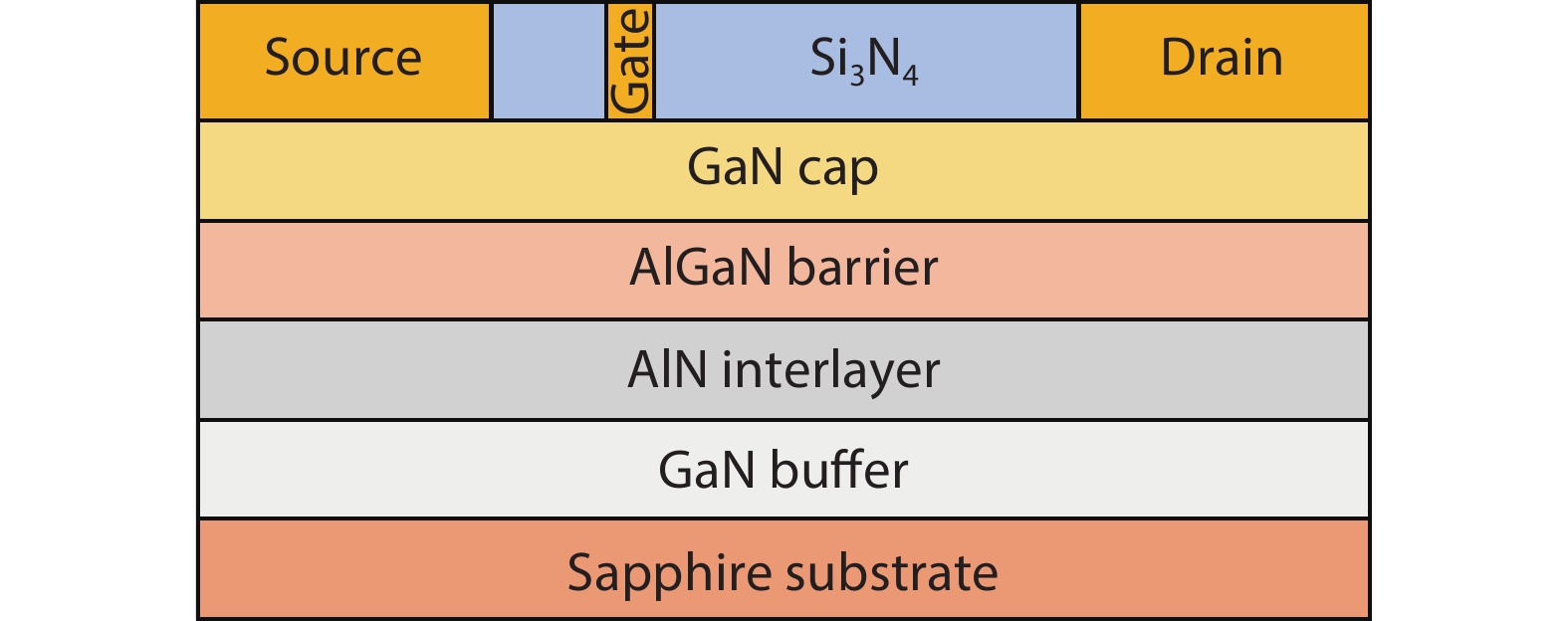
    Fig. 1. (Color online) The cross-section schematic of the AlGaN/GaN HEMT.
    (Color online) Reverse I–V characteristics measured from 298 to 458 K in a step of 40 K of (a) unannealed HEMT, (b) annealed HEMT.
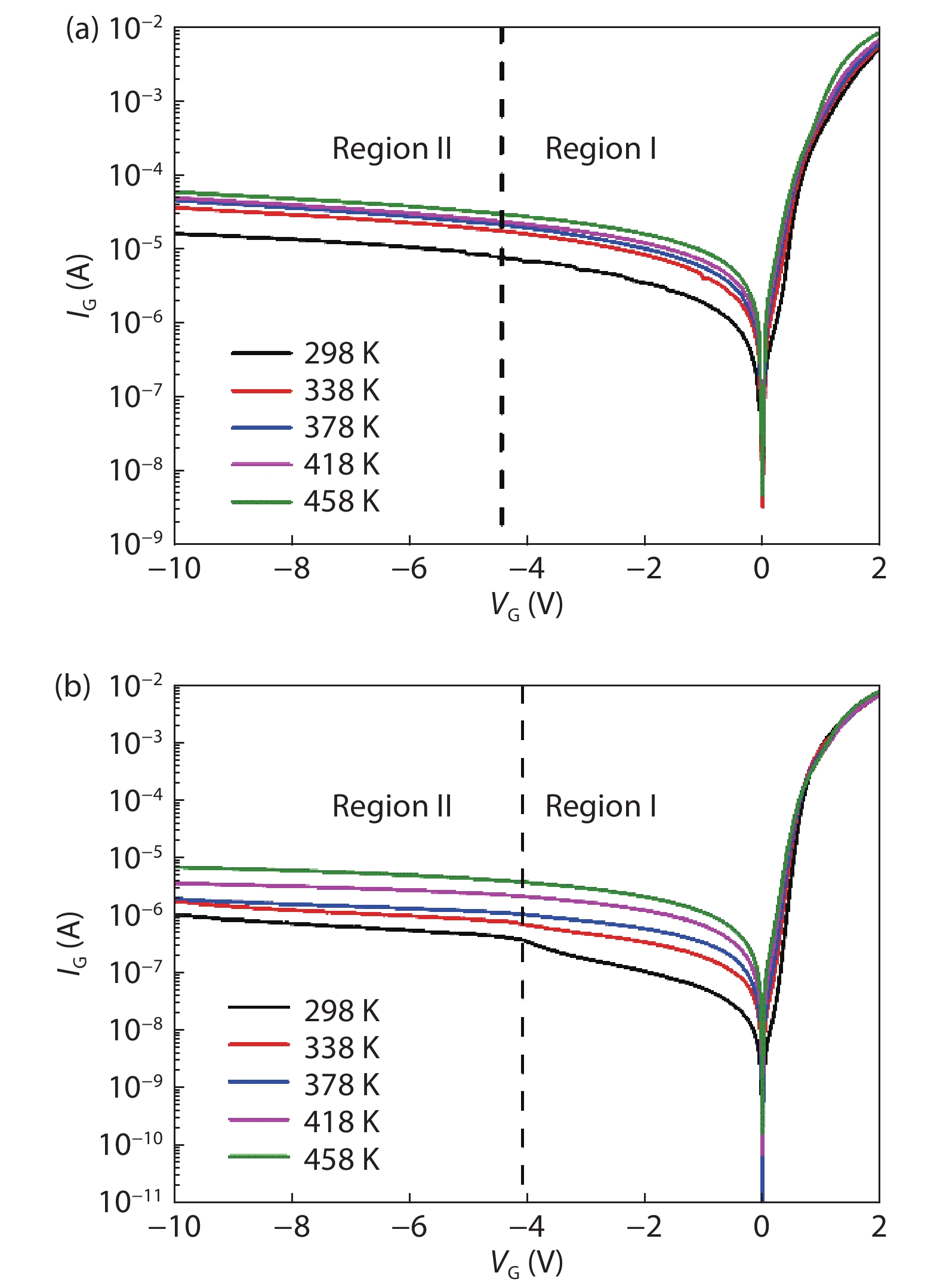
    Fig. 2. (Color online) Reverse I–V characteristics measured from 298 to 458 K in a step of 40 K of (a) unannealed HEMT, (b) annealed HEMT.
    (Color online) (a) The gate capacitance versus VG characteristics of both HEMTs. (b) The electric fields across AlGaN as the function of VG for both HEMTs.
    Fig. 3. (Color online) (a) The gate capacitance versus VG characteristics of both HEMTs. (b) The electric fields across AlGaN as the function of VG for both HEMTs.
    (Color online) The ln (J/E) versus E0.5 and the linear fit for the slope and intercepts of (a) unannealed HEMT, (b) annealed HEMT. Inset: the B(T) versus for the extraction of the height of the trap state.
    Fig. 4. (Color online) The ln (J/E) versus E0.5 and the linear fit for the slope and intercepts of (a) unannealed HEMT, (b) annealed HEMT. Inset: the B(T) versus for the extraction of the height of the trap state.
    (Color online) Gate leakage measured during the reverse gate-bias step stress of (a) unannealed HEMT, (b) annealed HEMT. Inset: absolute value of reverse gate-bias step stress versus times (Vstep = –5 V, tstep = 60 s).
    Fig. 5. (Color online) Gate leakage measured during the reverse gate-bias step stress of (a) unannealed HEMT, (b) annealed HEMT. Inset: absolute value of reverse gate-bias step stress versus times (Vstep = –5 V, tstep = 60 s).
    (Color online) Gate leakage current before and after reverse bias step stress of (a) unannealed HEMT, (b) annealed HEMT, (c) maximum output currents, and (d) transfer characteristics before and after reverse bias step stress of the unannealed HEMT.
    Fig. 6. (Color online) Gate leakage current before and after reverse bias step stress of (a) unannealed HEMT, (b) annealed HEMT, (c) maximum output currents, and (d) transfer characteristics before and after reverse bias step stress of the unannealed HEMT.
    (Color online) Schematic of the gate leakage at reverse gate bias before the stress of (a) unannealed HEMT, (b) annealed HEMT.
    Fig. 7. (Color online) Schematic of the gate leakage at reverse gate bias before the stress of (a) unannealed HEMT, (b) annealed HEMT.
    Changxi Chen, Quan Wang, Wei Li, Qian Wang, Chun Feng, Lijuan Jiang, Hongling Xiao, Xiaoliang Wang. Effect of the post-gate annealing on the gate reliability of AlGaN/GaN HEMTs[J]. Journal of Semiconductors, 2021, 42(9): 092802
    Download Citation