
Changxi Chen, Quan Wang, Wei Li, Qian Wang, Chun Feng, Lijuan Jiang, Hongling Xiao, Xiaoliang Wang. Effect of the post-gate annealing on the gate reliability of AlGaN/GaN HEMTs[J]. Journal of Semiconductors, 2021, 42(9): 092802
- Journal of Semiconductors
- Vol. 42, Issue 9, 092802 (2021)
Abstract
1. Introduction
In recent years, AlGaN/GaN high electron mobility transistors (HEMTs) have attracted a lot of attention, owing to their excellent properties for high-power and high-frequency applications[
In the off-state biased HEMTs, the inverse piezoelectric effect or gate degradation will appear if the applied bias exceeds the so-called “critical voltage”, which is often obtained by performing reverse bias step-stress experiments. The inverse piezoelectric effect and gate degradation are respectively related to the formation of crystallographic defects due to the strain relaxation[
In this paper, temperature-dependent current–voltage characteristics were carried out to investigate the reverse leakage mechanism of HEMTs at low reverse gate bias before and after the PGA process. Furthermore, the Schottky gate reliability of the unannealed and annealed HEMTs were studied by the reverse step stress and the reverse gate leakage currents of both HEMTs after the step-stress were compared and analyzed.
2. Experiment
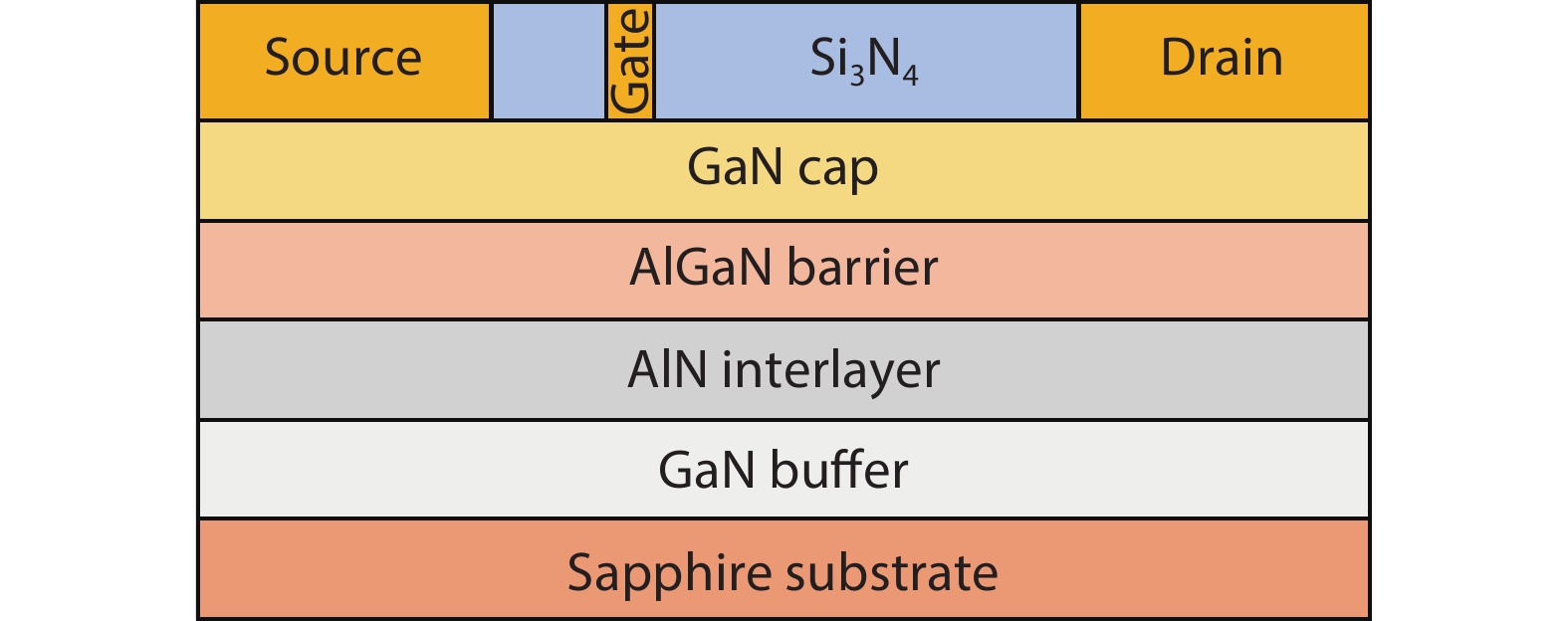
The AlGaN/GaN HEMT structures were grown on a 2-inch sapphire substrate by metal organic chemical vapor deposition (MOCVD). The epitaxial structure consists of a 3 μm GaN buffer layer, a 1 nm AlN insertion layer, a 20 nm Al0.23Ga0.77N barrier layer, and a 3 nm GaN cap layer, as shown in Fig. 1. Ohmic metallization Ti/Al/Ti/Au (20/100/40/50 nm) were first deposited, and annealed in a N2 atmosphere at 870 °C for 30 s. The specific resistivity was 1 × 10⁻⁵ Ω·cm2 calculated by the transmission line method (TLM). The devices isolation was conducted by inductively coupled plasma (ICP) dry etching with an etch depth of 180 nm. Ni/Au (40/200 nm) metallization were sputtered and lifted off to form the Schottky gate. Finally, the devices were passivated by a 200 nm thick Si3N4 layer deposited by plasma enhanced chemical vapor deposition (PECVD). The gate length, gate width, spacing of gate to drain, and spacing of the gate to source are 3, 100, 20, 5 μm, respectively. To optimize the post-gate-annealing condition, the wafer was cleaved to several pieces after fabrication accomplishment. The annealing temperature was chosen to be 400 °C as referred from the works[
![]()
Figure 1.(Color online) The cross-section schematic of the AlGaN/GaN HEMT.
3. Results and discussion
To investigate the reverse gate leakage mechanisms of the unannealed and annealed HMETs, the gate I–V characteristics at different temperatures (from 298 to 458 K with a step of 40 K) of both HEMTs are shown in Fig. 2. The reverse gate leakage currents are dependent both on the bias and temperature at low reverse bias (Vth < VG < 0 V, region I), and become nearly saturated at high reverse bias ( VG < Vth, region II). This indicates that the leakage current in region I plays a very significant role in gate reverse leakage. Besides, it is found that the reverse gate leakage currents is reduced significantly after the PGA, as shown in Figs. 2(a) and 2(b).
![]()
Figure 2.(Color online) Reverse
Since many reverse leakage mechanisms are related to the electric fields across the AlGaN barrier layer[
where σp is the net polarization charge density at the AlGaN/GaN interface, including the piezoelectric polarization charge and spontaneous polarization charge at the AlGaN/GaN interface, ns is the two-dimensional electronic gas (2DEG) density at the hetero-structure and εr is the relative dielectric constant of the AlGaN barrier. The value of σp used in Eq. (1) is set to 1.3 × 1013 cm–2[
The ns as the function of gate voltage can be calculated by high frequency C–V measurement. In Fig. 3(a), the gate capacitance versus gate voltage characteristics of both HEMTs are depicted. Subsequently, the corresponding ns is obtained by integrating the C–V curve of a gate diode. Thus, the electric fields across AlGaN barriers as the function of gate voltages for both HEMTs are obtained, as shown in Fig. 3(b). At low reverse bias, the electric fields increase with the bias voltages linearly, and become constant when the voltages reach their critical values. The constant electric field comes from the net polarization charges at the AlGaN/GaN interface, due to the total depletion of the 2DEG. In fact, the turning points in Fig. 3(b) represent the threshold voltages of the unannealed and annealed HEMTs, respectively. As can be seen, the threshold voltage of AlGaN/GaN HEMT exhibits a positive shift after the PGA, which can be attributed to the reduction of the electron density under the gate[
![]()
Figure 3.(Color online) (a) The gate capacitance versus
Because the Poole–Frenkel emission is one of the most common leakage mechanisms at low reverse bias, which is field-dependent as well as temperature-dependent[
The current density–electric field (J–E) of PF emission can be expressed by follows[
where A is a constant,
where
If the leakage current is dominated by the PF emission at low gate voltage, Eq. (3) points out that
![]()
Figure 4.(Color online) The ln (
In order to study the effects of the PGA on the gate reliability of HEMTs, reverse gate bias step stresses were carried out for the unannealed and annealed HEMTs. As shown in the inset of Fig. 5(a), the gate stress is stepped from –5 to –45 V in a –5 V increment for 60 s per step with the drain and source grounded. In Figs. 5(a) and 5(b), gate leakage current (IG), source leakage current (IGS) and drain leakage current (IGD) of both devices are displayed, respectively, where the IG is the sum of IGS and IGD. In Fig. 5(a), three types of the leakage current rise abruptly at different positions, which correspond to the “degradation voltages”. The absolute values of the degradation voltage for IG and IGS are 35 V, which are lower than 40 V for IGD. This suggests that the gate degradation starts at the source edge near the gate, owing to shorter spacing of the gate to the source. Nevertheless, the gate leakage current of the annealed HEMT increases slowly with the reverse gate voltage, shown in Fig. 5(b), and there is no sharp increase in the three types of currents during the gate stress. The early gate degradation of the unannealed HEMT indicates that the higher initial gate leakage current will accelerate the gate degradation.
![]()
Figure 5.(Color online) Gate leakage measured during the reverse gate-bias step stress of (a) unannealed HEMT, (b) annealed HEMT. Inset: absolute value of reverse gate-bias step stress versus times (
For further studying the gate degradation of unannealed and annealed HEMTs, the gate leakage currents before and after reverse step stress for both HEMTs are exhibited in Figs. 6(a) and 6(b). Before the step stress, the reverse gate leakage current of the unannealed HEMT is higher than that of the annealed HEMT, owing to the lower PF emission barrier. After the step stress, the reverse gate leakage current of the unannealed HEMT increases significantly, and it could not recover even waiting for 24 h. Therefore, there must be some new leaking path generated below the gate/AlGaN interface, beneficial for the electrons transporting from the gate to the channel. Conversely, the reverse gate leakage of the annealed HEMT only changes slightly after the gate stress, indicating the improved reliability of the Schottky gate in the annealed HEMT. Additionally, the maximum output currents and the transfer characteristics of the unannealed HEMT before and after the reverse-bias step stress are shown in Figs. 6(c) and 6(d). The maximum output current and the transfer characteristic can almost recover within 5 min after the stress except the leakage current in the pinch-off region. This indicates that the permanent gate damage in the unannealed HEMT after the step stress cannot be attributed to the converse piezoelectric effect, which is associated with the creation of macro-defect as reported in Ref. [24].
![]()
Figure 6.(Color online) Gate leakage current before and after reverse bias step stress of (a) unannealed HEMT, (b) annealed HEMT, (c) maximum output currents, and (d) transfer characteristics before and after reverse bias step stress of the unannealed HEMT.
To better explain the mechanisms of the gate leakage before the reverse step stress for the unannealed and annealed HEMTs, the conduction band diagrams of both HEMTs are depicted in Fig. 7. As labeled by the blue dash-dot line, a continuum of states is presented in the material, which is related to the conductive dislocations in the barrier layer. Electrons can be activated by thermal energy from a trap state to a continuum of states. At low reverse gate bias (Vth < VG < 0), the barrier of the emission from the trap state to a continuum of states lowers with the increase of electric field [
![]()
Figure 7.(Color online) Schematic of the gate leakage at reverse gate bias before the stress of (a) unannealed HEMT, (b) annealed HEMT.
4. Conclusion
In summary, the gate leakage mechanisms at low reverse gate bias and the gate reliability of HEMTs before and after the PGA have been investigated. At the low reverse bias region, the PF emission is dominant in gate leakage of the unannealed and annealed HEMTs. Before the step stress, the gate leakage current is reduced by more than one order in the annealed HEMT, since the emission barrier height is increased from 0.139 to 0.256 eV by the PGA process. In a reverse step-stress experiment, the unannealed HMET exhibits an irreversible degradation at low reverse voltage (VG = –35 V), indicating the permanent gate degradation. After the gate stress, the gate leakage current of the unannealed HEMT becomes higher, while the gate leakage current of the annealed HEMT remains almost unchanged. The experimental results suggest that the PGA is an effective method to reduce the reverse gate leakage current and improve the reliability of the gate for the AlGaN/GaN HEMTs.
Acknowledgements
This work was supported by the National Key Research and Development Program of China (2017YFB0402900) and the National Natural Sciences Foundation of China (62074144).
References
[1] S Wu, X H Ma, L Yang et al. A millimeter-wave AlGaN/GaN HEMT fabricated with transitional-recessed-gate technology for high-gain and high-linearity applications. IEEE Electron Device Lett, 40, 846(2019).
[2] J S Moon, J Wong, B Grabar et al. 360 GHz
[3] P Murugapandiyan, S Ravimaran, J William et al. Design and analysis of 30 nm T-gate InAlN/GaN HEMT with AlGaN back-barrier for high power microwave applications. Superlattices Microstruct, 111, 1050(2017).
[4] Y Q Chen, X Y Liao, C Zeng et al. Degradation mechanism of AlGaN/GaN HEMTs during high temperature operation stress. Semicond Sci Technol, 33, 015019(2018).
[5] J A del Alamo, J Joh. GaN HEMT reliability. Microelectron Reliab, 49, 1200(2009).
[6] Z Gao, F Rampazzo, M Meneghini et al. Degradation mechanism of 0.15
[7] D Marcon, T Kauerauf, F Medjdoub et al. A comprehensive reliability investigation of the voltage-, temperature- and device geometry-dependence of the gate degradation on state-of-the-art GaN-on-Si HEMTs. 2010 International Electron Devices Meeting, 20.3.1(2010).
[8] S Sudharsanan, S Karmalkar. Modeling of the reverse gate leakage in AlGaN/GaN high electron mobility transistors. J Appl Phys, 107, 064501(2010).
[9] R Jos. Reverse Schottky gate current in AlGaN-GaN high-electron-mobility-transistors. J Appl Phys, 112, 094508(2012).
[10] H Zhang, E J Miller, E T Yu. Analysis of leakage current mechanisms in Schottky contacts to GaN and Al0.25Ga0.75N∕GaN grown by molecular-beam epitaxy. J Appl Phys, 99, 023703(2006).
[11] S Turuvekere, D S Rawal, A DasGupta et al. Evidence of Fowler–Nordheim tunneling in gate leakage current of AlGaN/ GaN HEMTs at room temperature. IEEE Trans Electron Devices, 61, 4291(2014).
[12] J Kotani, M Tajima, S Kasai et al. Mechanism of surface conduction in the vicinity of Schottky gates on AlGaN∕GaN heterostructures. Appl Phys Lett, 91, 093501(2007).
[13] S Zhang, X Y Liu, K Wei et al. Suppression of gate leakage current in ka-band AlGaN/GaN HEMT with 5-nm SiN gate dielectric grown by plasma-enhanced ALD. IEEE Trans Electron Devices, 68, 49(2021).
[14] K Kim, T J Kim, H L Zhang et al. AlGaN/GaN Schottky-gate HEMTs with UV/O3-treated gate interface. IEEE Electron Device Lett, 41, 1488(2020).
[15] L Liu, Y Y Xi, S Ahn et al. Characteristics of gate leakage current and breakdown voltage of AlGaN/GaN high electron mobility transistors after postprocess annealing. J Vac Sci Technol B, 32, 052201(2014).
[16] H Kim, J Lee, D M Liu et al. Gate current leakage and breakdown mechanism in unpassivated AlGaN∕GaN high electron mobility transistors by post-gate annealing. Appl Phys Lett, 86, 143505(2005).
[17] E V Sleptsov, A V Chernykh, S V Chernykh et al. Investigation of the thermal annealing effect on electrical properties of Ni/Au, Ni/Mo/Au and Mo/Au Schottky barriers on AlGaN/GaN heterostructures. J Phys: Conf Ser, 816, 012039(2017).
[18] A K Visvkarma, R Laishram, S Kapoor et al. Improvement in DC and pulse characteristics of AlGaN/GaN HEMT by employing dual metal gate structure. Semicond Sci Technol, 34, 105013(2019).
[19] D W Yan, H Lu, D S Cao et al. On the reverse gate leakage current of AlGaN/GaN high electron mobility transistors. Appl Phys Lett, 97, 153503(2010).
[20] M L Hao, Q Wang, L J Jiang et al. Gate leakage and breakdown characteristics of AlGaN/GaN high-electron-mobility transistors with Fe delta-doped buffer. Nanosci Nanotechnol Lett, 10, 185(2018).
[21] Z J Lin, H Kim, J Lee et al. Thermal stability of Schottky contacts on strained AlGaN/GaN heterostructures. Appl Phys Lett, 84, 1585(2004).
[22] S Turuvekere, N Karumuri, A A Rahman et al. Gate leakage mechanisms In AlGaN/GaN and AlInN/GaN HEMTs: Comparison and modeling. IEEE Trans Electron Devices, 60, 3157(2013).
[23] H Kim, M L Schuette, J Lee et al. Passivation of surface and interface states in AlGaN/GaN HEMT structures by annealing. J Electron Mater, 36, 1149(2007).
[24] D Marcon, J Viaene, P Favia et al. Reliability of AlGaN/GaN HEMTs: Permanent leakage current increase and output current drop. Proceedings of the 20th IEEE International Symposium on the Physical and Failure Analysis of Integrated Circuits (IPFA), 249(2013).
[25] C Y Chang, E A Douglas, J Kim et al. Electric-field-driven degradation in off-state step-stressed AlGaN/GaN high-electron mobility transistors. IEEE Trans Device Mater Reliab, 11, 187(2011).
[26] M Meneghini, A Stocco, M Bertin et al. Time-dependent degradation of AlGaN/GaN high electron mobility transistors under reverse bias. Appl Phys Lett, 100, 033505(2012).

Set citation alerts for the article
Please enter your email address
© Copyright 2018-2021 | Chinese Laser Press. All Rights Reserved 沪ICP备15018463号-20