
Hailong Wang, Jialin Ma, Qiqi Wei, Jianhua Zhao. Mn doping effects on the gate-tunable transport properties of Cd3As2 films epitaxied on GaAs[J]. Journal of Semiconductors, 2020, 41(7): 072903
- Journal of Semiconductors
- Vol. 41, Issue 7, 072903 (2020)
Abstract
1. Introduction
As a representative material of topological Dirac semimetal (TDS), Cd3As2 has been intensively studied in recent years thanks to its stability in air and its high carrier mobility[
Efficient methods to break the symmetry include introducing strain through lattice mismatch or piezo-electric substrate, or by doping magnetic elements[
In this work, we investigate the symmetry breaking effects on the transport properties of Cd3As2 films by introducing lattice strain and magnetic element doping. Specifically, Mn-doped Cd3As2 films are directly grown on semi-insulating GaAs(111)B substrates by low temperature molecular-beam epitaxy (LT-MBE). Mn concentration higher than 2% would easily cause the generation of second phase, which might be attributed to the large lattice mismatch between GaAs and Cd3As2. Shubnikov-de Haas (SdH) oscillation and quantum Hall effect are observed at low temperatures, and electrons are found to be the dominant carrier, both at room temperature and low temperature. Larger Mn content leads to smaller lattice constant, lower electron mobility, and larger effective band gap, while the electron density seems to be unaffected by Mn-doping. Gating experiments show that SdH oscillation and QHE can be slightly modulated by electric field, which is ascribed to the variation of carrier density. Our results are valuable for the study of the magnetic element doping effects on the physical properties of Cd3As2 films.
2. Epitaxial growth of Mn-doped Cd3As2 films
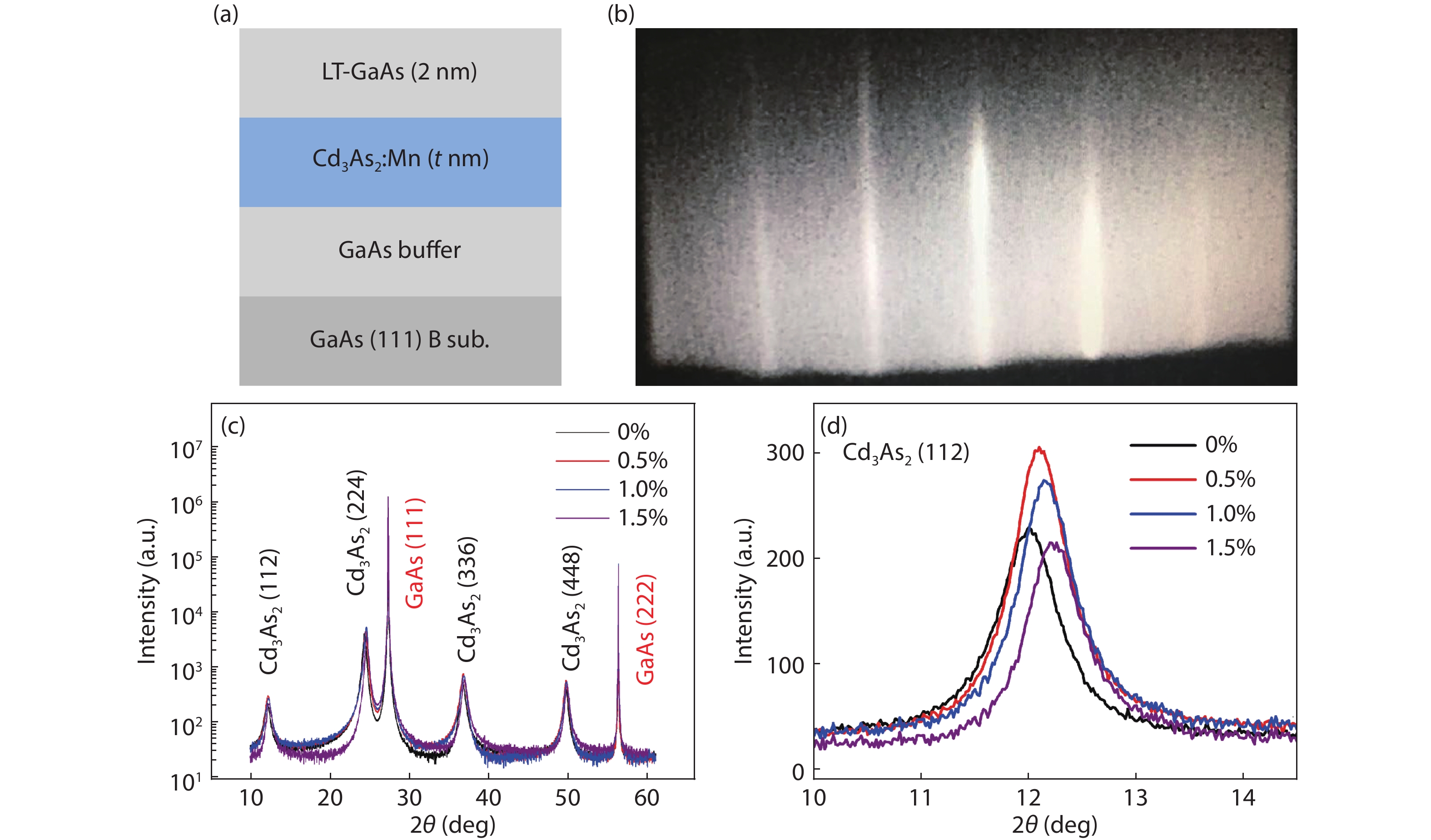
A series of Cd3As2 films with different Mn doping concentration were grown on epi-ready GaAs(111)B substrates, during which the molecular beams of Cd, Mn and As were separately controlled by using three isolated effusion cells. The GaAs buffer layer was deposited at high temperature (560 °C), and the following Mn-doped Cd3As2 films and GaAs capping layer (for the aim of avoiding oxidation of Cd3As2) was grown at low temperature (180 °C). The growth process was monitored by reflection high-energy electron diffraction (RHEED), and streaky patterns of Cd3As2 films could be observed and used to infer the orientation of the crystal plane, as shown in Fig. 1(b). The growth window of Cd3As2 films is quite narrow, with the growth temperature in the range from 170 to 200 °C and nominal Cd/As ratio of 0.7 to 3.5. The incorporation of Mn does not obviously affect the growth conditions, and no signature of second phase would appear if the Mn content is less than 2%. When the thickness of the Mn-doped Cd3As2 film exceeds 150 nm, the brightness of the RHEED patterns would gradually weaken. Therefore, we will focus on the samples with thickness ranging from 10 to 100 nm, and only the samples with good crystal quality as judged by their XRD and RHEED data will be selected for further investigations. Notice the atoms in Cd3As2 (112) arrange themselves in the form of a quasi-hexagon, which explains the epitaxial mode of Cd3As2 (112) // GaAs (111) since the GaAs {111} planes are hexagonal as well[
![]()
Figure 1.(Color online) (a) Layer structure, (b) RHEED pattern, and (c) XRD curves of Cd3As2 films with various Mn doping concentration. (d) The enlarged XRD curves of (c) around the Cd3As2 (112) diffraction peak.
It should be mentioned that the RHEED patterns have a clear change during the transition from GaAs (111) to Cd3As2 (112) (corresponding to the process for depositing ~1 nm thick Cd3As2), and then kept nearly the same. This suggests a rapid relaxation of Cd3As2 lattices, although the lattice mismatch between Cd3As2 and GaAs is quite large.
Fig. 1(c) shows the X-ray diffraction (XRD) results of Cd3As2 films (50 nm) with Mn doping concentration of 0%, 0.5%, 1.0% and 1.5%, respectively. In the diffraction angles (2θ) range of 10° to 60°, four peaks corresponding to the Cd3As2 (112), (224), (336) and (448) crystal planes could also be identified, in addition to the strong GaAs (111) and (222) diffraction peaks. The calculated lattice constants from XRD results are similar with the bulk values, confirming the quick relaxation of the Cd3As2 films. This is similar to the results of Cd3As2 films grown on GaSb (111) or CdTe buffer layer by LT-MBE, where the lattice mismatch is also not negligible[
3. Transport properties of Mn-doped Cd3As2 films
The Cd3As2 samples were fabricated into top-gated field-effect devices, the structure is schematically shown in Fig. 2(a). After the 30 μm wide Hall bar was defined with Cd3As2 as the channel via optical lithography and ion-beam milling, a 50 nm thick Al2O3 insulating layer was deposited onto the sample at 80 °C by atomic layer deposition (ALD). Finally, an Au/Cr electrode was formed using thermal evaporation and lift-off processes. The electric current was applied along the GaAs [11-2] direction, and the distance between nearby electrodes is 30 μm. To efficiently modulate the transport properties by electric field, relatively thin Cd3As2 films (20 nm) were chosen. Temperature dependence of the longitudinal resistance curves (Rxx–T) without applying magnetic field are plotted in Fig. 2(b). Clearly, the four samples with different Mn doping concentration all exhibit semiconductor-like temperature dependency at high temperatures, consistent with the theoretical prediction and previous experimental reports of Cd3As2 films grown by MBE[
![]()
Figure 2.(Color online) (a) Field effect device diagram, (b) Temperature dependence, and (c, d) Magnetic field dependence of Mn-doped Cd3As2 films. The inset of (b) shows the fitting line based on Arrhenius equation, in which the blue curve is offset for clarity.
where Ea and kB are the activation energy and Boltzmann constant, respectively. The activation energy can be extrapolated, as shown in the inset of Fig. 2(b)[
The magnetoresistance (MR) curves at 300 K with magnetic field (B) perpendicular to the plane are presented in Fig. 2(c). For this geometric configuration, the positive MR at room temperature changes as a parabolic curve in the low magnetic field region (B < ~4 T), and shows linear dependence in the high magnetic field region. This is quite different from the results of undoped bulk materials, in which linear MR dominates in a large magnetic field range (up to 14.5 T) at high temperatures [
When the temperature was lowered down to 2 K, clear SdH oscillation can be observed for all the samples except the 2% Mn-doped one, as shown in Fig. 2(d). In contrast to the positive MR at 300 K, the MR at 2 K is negative for all the four samples. The amplitude of the SdH oscillations decreases with increasing the Mn concentration, which is an indication of the decreasing electron mobility due to the enhanced magnetic scattering. This result is very different from the previous reports on Cd3As2 films with thickness of 100 nm, in which the gap opening effect was thought to be insignificant[
In Fig. 3(a), the Hall resistance as a function of magnetic field (Rxy–B) at 300 K is presented. As can be seen from the negative slope in the whole magnetic field range, the transport behavior is mainly determined by electron. We notice that two-carrier transport was reported for Cd3As2 films with thickness larger than 50 nm and ~350 nm thick nanoplates, where the Hall resistance was curved due to the competing contributions of electrons and holes[
![]()
Figure 3.(Color online) Hall resistance as a function of magnetic field in Mn-doped Cd3As2 films at (a) 300 K and (b) 2 K. The unit of (b) is
Fig. 3(b) shows the Rxy–B at 2 K, in which QHE was observed in non-doped and moderately Mn-doped Cd3As2 films. Similarly, the negative slope in the low field region gives the sheet electron density of 9.7 (8.6, 11.3 and 10.5) ×1011 cm–2 for the 0% (0.5%, 1.0% and 1.5%) Mn-doped sample, consistent with the results derived from the SdH oscillation. The electron density at 2 K is several times smaller than that at 300 K, which can be explained by the thermal excitation of carriers. The electron mobility is 3267 (2659, 1785 and 972) cm2/(V·s), about 5.2 (5.4, 5.0 and 4.7) times larger than the room temperature values. The mobility is much lower than the bulk case, but is comparable with films grown on CdTe/mica or GaSb/GaAs substrates[
4. Electric-field modulation of the transport properties
Because of the narrow band gap and small density of states at the conduction and valence band edges, it should be relatively easy to shift Fermi energy and thus affect the carrier density. Therefore, we employ the electric field to manipulate the transport properties of the Mn-doped Cd3As2 films, and the main results are shown in Fig. 4. The gate voltage is applied by a Keithley 2400 source-meter, whose polarity is defined with respect to the channel.
![]()
Figure 4.(Color online) Magnetic field dependence of (a) longitudinal and (b) transverse resistances for a 0.5% Mn-doped Cd3As2 film at 2 K.
Fig. 4(a) shows the MR curves of the 0.5% Mn-doped sample modulated by gate voltages at 2 K, from which slight shifts of the SdH oscillation peaks can be identified. Electrons will be accumulated inside the Cd3As2 films by applying positive voltage, and depleted by negative gate voltage. The change of sheet electron density could be calculated by Δns = ε0εΔEG/e, where ε0, ε, e and ΔEG are the electric constant, relative electric permittivity (~7 for Al2O3), the elementary charge and changing amount of gate electric field, respectively. The variation of electron density leads to a corresponding change of the SdH oscillation, as the period is characterized by its inverse in the form of Δ(1/B) = 2e/(hns), where h is the Planck constant. According to this equation, a positive (negative) gate voltage of 5 V would change the period of 0.056 T–1 to 0.0051 (0.0080) T–1. The corresponding values obtained from the experimental data are 0.039 T–1 and 0.063 T–1 under positive and negative gate voltages, which do not change too much compared with the above estimation. Usually, this large inconsistency is caused by the high-density interface states, which screen the gate electric field from penetrating the Cd3As2 films. In our case, the screening is mainly caused by the interface between GaAs and Cd3As2, since our previous works on GaAs/(Ga,Mn)As show that the surface states of GaAs capping layer facing to the Al2O3 layer can be ignored[
The corresponding change of the Hall resistance is plotted in Fig. 4(b), and the QHE plateau shifts when the gate voltage is varied from 5 to –5 V. Again, the electron density deduced from the slope of the low field data is consistent with the one determined by the SdH oscillation, verifying the gating effect in this sample.
5. Conclusion
In conclusion, by introducing lattice strain and magnetic element doping, we investigate the symmetry breaking effects on the transport properties of Mn-doped Cd3As2 films grown on semi-insulating GaAs(111)B substrate. Larger Mn content results in a smaller lattice constant, lower electron mobility, and larger effective band gap, while the electron density seems to be independent of the Mn-doping concentration. Gating experiments show that SdH oscillation and QHE can be slightly modulated by electric field, which is ascribed to the variation of carrier density. Our results are valuable for the study of the magnetic elements doping effects on the physical properties of Cd3As2 films.
Acknowledgements
This work is supported by NSFC (Grants Nos. U1632264 and 11704374), and the the Strategic Priority Research Program of the Chinese Academy of Sciences (Grant Nos. XDB44000000 and QYZDY-SSW-JSC015).
References
[1] Z J Wang, H M Weng, Q S Wu et al. Three-dimensional Dirac semimetal and quantum transport in Cd3As2. Phys Rev B, 88, 125427(2013).
[2] M N Ali, Q Gibson, S Jeon et al. The crystal and electronic structures of Cd3As2, the three-dimensional electronic analogue of graphene. Inorg Chem, 53, 4062(2014).
[3] S Borisenko, Q Gibson, D Evtushinsky et al. Experimental realization of a three-dimensional Dirac semimetal. Phys Rev Lett, 113, 027603(2014).
[4] Z K Liu, J Jiang, B Zhou et al. A stable three-dimensional topological Dirac semimetal Cd3As2. Nat Mater, 13, 677(2014).
[5] S Jeon, B B Zhou, A Gyenis et al. Landau quantization and quasipartical interference in the three-dimensional Dirac semimetal Cd3As2. Nat Mater, 13, 851(2014).
[6] M Neupane, S Y Xu, R Sankar et al. Observation of a three-dimensional topological Dirac semimetal phase in high-mobility Cd3As2. Nat Commun, 5, 3786(2014).
[7] A C Potter, I Kimchi, A Vishwanath. Quantum oscillations from surface Fermi arcs in Weyl and Dirac semimetals. Nat Commun, 5, 5161(2014).
[8] L P He, X C Hong, J K Dong et al. Quantum transport evidence for the three-dimensional Dirac semimetal phase in Cd3As2. Phys Rev Lett, 113, 246402(2014).
[9] T Liang, Q Gibson, M N Ali et al. Ultrahigh mobility and giant magnetoresistance in the Dirac semimetal Cd3As2. Nat Mater, 14, 280(2015).
[10] Y F Zhao, H W Liu, C L Zhang et al. Anisotropic Fermi surface and quantum limit transport in high mobility three-dimensional Dirac semimetal Cd3As2. Phys Rev X, 5, 031037(2015).
[11] Z J Jiang, D Zhao, Z Jin et al. Angular-dependent phase factor of Shubnikov-de Haas oscillations in the Dirac semimetal Cd3As2. Phys Rev Lett, 115, 226401(2015).
[12] P J W Moll, N L Nair, T Helm et al. Transport evidence for Fermi-arc-mediated chirality transfer in the Dirac semimetal Cd3As2. Nature, 535, 366(2016).
[13] C Zhang, A Narayan, S H Lu et al. Evolution of Weyl orbit and quantum Hall effect in Dirac semimetal Cd3As2. Nat Commun, 8, 1272(2017).
[14] C M Wang, H P Sun, H Z Lu et al. 3D quantum Hall effect of Fermi arcs in topological semimetals. Phys Rev Lett, 119, 136806(2017).
[15] M Uchida, Y Nakazawa, S Nishihaya et al. Quantum Hall states observed in thin films of Dirac semimetal Cd3As2. Nat Commun, 8, 2274(2017).
[16] T Schumann, L Galletti, D A Kealhofer et al. Observation of the quantum Hall effect in confined films of the three-dimensional Dirac semimetal Cd3As2. Phys Rev Lett, 120, 016801(2018).
[17] M Goyal, L Galletti, S Salmani-Rezaie et al. Thickness dependence of the quantum Hall effect in films of the three-dimensional Dirac semimetal Cd3As2. APL Mater, 6, 026105(2018).
[18] C Zhang, Y Zhang, X Yuan et al. Quantum Hall effect based on Weyl orbits in Cd3As2. Nature, 331, 565(2019).
[19] B C Lin, S Wang, S Wiedmann et al. Observation of an odd-integer quantum Hall effect from topological surface states in Cd3As2. Phys Rev Lett, 122, 036602(2019).
[20] Y Zhang, C Zhang, H X Gao et al. Large Hall angle-driven magneto-transport phenomena in topological Dirac semimetal Cd3As2. Appl Phys Lett, 113, 072104(2018).
[21] S Nishihaya, M Uchida, Y Nakazawa et al. Quantized surface transport in topological Dirac semimetal films. Nat Commun, 10, 2564(2019).
[22] C Z Li, L X Wang, H W Liu et al. Giant negative magnetoresistance induced by the chiral anomaly in individual Cd3As2 nanowires. Nat Commun, 6, 10137(2015).
[23] H Li, H T He, H Z Lu et al. Negative magnetoresistance in Dirac semimetal Cd3As2. Nat Commun, 7, 10301(2016).
[24] L Aggarwal, A Gaurav, G S Thakur et al. Unconventional superconductivity at mesoscopic point contacts on the 3D Dirac semimetal Cd3As2. Nat Mater, 15, 32(2016).
[25] H Wang, H C Wang, H W Liu et al. Observation of superconductivity induced by a point contact on 3D Dirac semimetal Cd3As2 crystals. Nat Mater, 15, 38(2016).
[26] A Q Wang, C Z Li, C Li et al. 4π-periodic supercurrent from surface states in Cd3As2 nanowire-based Josephson junctions. Phys Rev Lett, 121, 237701(2018).
[27] C Huang, B T Zhou, H Q Zhang et al. Proximity-induced surface superconductivity in Dirac semimetal Cd3As2. Nat Commun, 10, 2217(2019).
[28] L X Wang, C Z Li, D P Yu et al. Aharonov-Bohm oscillations in Dirac semimetal Cd3As2 nanowires. Nat Commun, 7, 10769(2016).
[29] L X Wang, S Wang, J G Li et al. Universal conductance fluctuation in Dirac semimetal Cd3As2 nanowires. Phys Rev B, 94, 161402(2016).
[30] S Wang, B C Lin, W Z Zheng et al. Fano interference between bulk and surface states of a Dirac semimetal Cd3As2 nanowire. Phys Rev Lett, 120, 257701(2018).
[31] T Zhou, C Zhang, H S Zhang et al. Enhanced thermoelectric properties of the Dirac semimeatl Cd3As2. Inorg Chem Front, 3, 1637(2016).
[32] Z Z Jia, C Z Li, X Q Li et al. Thermoelectric signature of the chiral anomaly in Cd3As2. Nat Commun, 7, 13013(2016).
[33] C H Zhu, F Q Wang, Y F Meng et al. A robust and tunable mid-infrared optical switch enabled by bulk Dirac fermions. Nat Commun, 8, 14111(2017).
[34] Q S Wang, C Z Li, S F Ge et al. Ultrafast broadband photodetectors based on three-dimensional Dirac semimetal Cd3As2. Nano Lett, 17, 834(2017).
[35] Y W Liu, C Zhang, X Yuan et al. Gate-tunable quantum oscillations in ambipolar Cd3As2 thin films. NPG Asia Mater, 7, e221(2015).
[36] C Z Li, J G Li, L X Wang et al. Two-carrier transport induced Hall anomaly and large tunable magnetoresistance in Dirac semimetal Cd3As2 nanoplates. ACS Nano, 10, 6020(2016).
[37] M Goyal, H Kim, T Schumann et al. Surface states of strained thin films of the Dirac semimetal Cd3As2. Phys Rev Mater, 3, 064204(2019).
[38] H Jin, Y Dai, Y D Ma et al. The electronic and magnetic properties of transition-metal element doped three-dimensional topological Dirac semimetal Cd3As2. J Mater Chem C, 3, 3547(2015).
[39] Y W Liu, R Tiwari, A Narayan et al. Cr doping induced negative transverse magnetoresistance in Cd3As2 thin films. Phys Rev B, 97, 085303(2018).
[40] X Yuan, P H Chen, L Q Zhang et al. Direct observation of landau level resonance and mass generation in Dirac semimetal Cd3As2 thin films. Nano Lett, 17, 2211(2017).
[41] Y Sun, Y F Meng, R H Dai et al. Slowing down photocarrier relaxation in Dirac semimetal Cd3As2 via Mn doping. Opt Lett, 44, 4103(2019).
[42] V S Zakhvalinskii, T B Nikulicheva, E Lahderanta et al. Anomalous cyclotron mass dependence on the magnetic field and Berry’s phase in (Cd1–
[43] T Schumann, M Goyal, H Kim et al. Molecular beam epitaxy of Cd3As2 on a III–V substrate. APL Mater, 4, 126110(2016).
[44] Y Nakazawa, M Uchida, S Nishihaya et al. Molecular beam epitaxy of three-dimensionally thick Dirac semimetal Cd3As2 films. APL Mater, 7, 071109(2019).
[45] D A Kealhofer, H Kim, T Schumann. Basal-plane growth of cadmium arsenide by molecular beam epitaxy. Phys Rev Mater, 3, 031201(2019).
[46] H L Wang, J L Ma, X Z Yu et al. Electric-field assisted switching of magnetization in perpendicularly magnetized (Ga,Mn)As films at high temperatures. J Phys D, 50, 025003(2017).
[47] H L Wang, J L Ma, J H Zhao. Giant modulation of magnetism in (Ga,Mn)As ultrathin films via electric field. J Semicond, 40, 092501(2019).

Set citation alerts for the article
Please enter your email address
© Copyright 2018-2021 | Chinese Laser Press. All Rights Reserved 沪ICP备15018463号-20