• Opto-Electronic Advances
  • Vol. 4, Issue 9, 210017-1 (2021)
Ziwei Li*, Wen Yang, Ming Huang, Xin Yang, Chenguang Zhu, Chenglin He, Lihui Li, Yajuan Wang, Yunfei Xie, Zhuoran Luo, Delang Liang, Jianhua Huang, Xiaoli Zhu, Xiujuan Zhuang, Dong Li, and Anlian Pan
Author Affiliations
  • Key Laboratory for Micro-Nano Physics and Technology of Hunan Province, College of Materials Science and Engineering, School of Physics and Electronics, Hunan University, Changsha 410082, China
  • show less
    DOI: 10.29026/oea.2021.210017 Cite this Article
    Ziwei Li, Wen Yang, Ming Huang, Xin Yang, Chenguang Zhu, Chenglin He, Lihui Li, Yajuan Wang, Yunfei Xie, Zhuoran Luo, Delang Liang, Jianhua Huang, Xiaoli Zhu, Xiujuan Zhuang, Dong Li, Anlian Pan. Light-triggered interfacial charge transfer and enhanced photodetection in CdSe/ZnS quantum dots/MoS2 mixed-dimensional phototransistors[J]. Opto-Electronic Advances, 2021, 4(9): 210017-1 Copy Citation Text show less
    Schematic view and TEM characterizations of MoS2 monolayer and CdSe/ZnS QDs. (a) Schematic view of mixed-dimensional QD/MoS2 heterostructures on SiO2/Si substrate under the excitation of a laser. (b) High-resolution TEM (HRTEM) image of MoS2 monolayer with the scale bar of 5 nm. The inset shows the corresponding selected area electron diffraction (SAED) pattern, where the diffraction points are arranged in a hexagonal structure. (c) Enlarged FFT image of the marked area in a rectangular region in (b). The lattice spacing is 2.78 Å. (d) The AFM image of MoS2 monolayer with clear surface, and the height of MoS2 is observed to be 0.75 nm. Low-resolution (e) and high-resolution (f) TEM images of QD/MoS2 heterostructures, where scale bars are 100 nm and 20 nm, respectively. The red arrows and circles in (e) are QDs on MoS2 monolayer, and the orange arrows in (f) are the wrinkles of MoS2 flakes. (g) The HRTEM image of QD/MoS2 structures with a scale bar of 2 nm. Inset shows two sets of SAED patterns.
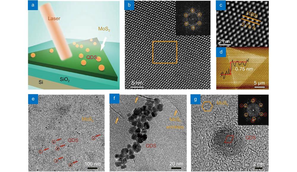
    Fig. 1. Schematic view and TEM characterizations of MoS2 monolayer and CdSe/ZnS QDs. (a) Schematic view of mixed-dimensional QD/MoS2 heterostructures on SiO2/Si substrate under the excitation of a laser. (b) High-resolution TEM (HRTEM) image of MoS2 monolayer with the scale bar of 5 nm. The inset shows the corresponding selected area electron diffraction (SAED) pattern, where the diffraction points are arranged in a hexagonal structure. (c) Enlarged FFT image of the marked area in a rectangular region in (b). The lattice spacing is 2.78 Å. (d) The AFM image of MoS2 monolayer with clear surface, and the height of MoS2 is observed to be 0.75 nm. Low-resolution (e) and high-resolution (f) TEM images of QD/MoS2 heterostructures, where scale bars are 100 nm and 20 nm, respectively. The red arrows and circles in (e) are QDs on MoS2 monolayer, and the orange arrows in (f) are the wrinkles of MoS2 flakes. (g) The HRTEM image of QD/MoS2 structures with a scale bar of 2 nm. Inset shows two sets of SAED patterns.
    Optical and spectral characteristics of QDs, MoS2 monolayer and mixed-dimensional vdWHs. (a) The UV-visible absorption spectrum (orange) of CdSe/ZnS QDs in 0.2 mg·L−1 solution. PL spectra of QDs in solution (blue) and on SiO2/Si substrate (dotted line). (b) Raman spectra of MoS2 monolayer and QD/MoS2 heterostructures. E12g and A1g modes are 384.2 cm−1 and 404.3 cm−1 for MoS2 monolayer, respectively, and the E12g peak shifts blue to 383.3 cm−1 in heterostructures. Insets present the optical microscopy images of MoS2 monolayer and heterostructure. The scale bars are 6 μm. (c) The absorption (black) and PL (red) spectra of MoS2 monolayer. The PL intensity maps of MoS2 monolayer are measured at the spectral ranges of (d) 665−750 nm and (e) 640−660 nm. The PL intensity maps of heterostructures with 0.025 mg·L−1 QDs are measured at the spectral ranges of (f) 665−750 nm and (g) 640−660 nm. All the scale bars in mapping images are 5 μm. (h) Time-resolved photoluminescence (TRPL) spectra of QDs and QD/MoS2 heterostructures. The average lifetimes of QDs and heterostrutures are 498.6 ps and 98.9 ps, respectively. (i) The schematic view of energy band for QD/MoS2 heterostructures under the light excitation.
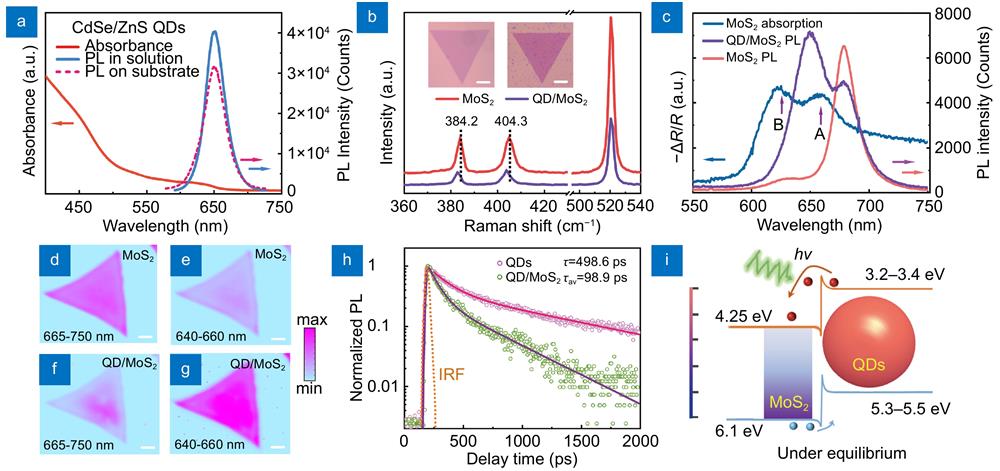
    Fig. 2. Optical and spectral characteristics of QDs, MoS2 monolayer and mixed-dimensional vdWHs. (a) The UV-visible absorption spectrum (orange) of CdSe/ZnS QDs in 0.2 mg·L−1 solution. PL spectra of QDs in solution (blue) and on SiO2/Si substrate (dotted line). (b) Raman spectra of MoS2 monolayer and QD/MoS2 heterostructures. E12g and A1g modes are 384.2 cm−1 and 404.3 cm−1 for MoS2 monolayer, respectively, and the E12g peak shifts blue to 383.3 cm−1 in heterostructures. Insets present the optical microscopy images of MoS2 monolayer and heterostructure. The scale bars are 6 μm. (c) The absorption (black) and PL (red) spectra of MoS2 monolayer. The PL intensity maps of MoS2 monolayer are measured at the spectral ranges of (d) 665−750 nm and (e) 640−660 nm. The PL intensity maps of heterostructures with 0.025 mg·L−1 QDs are measured at the spectral ranges of (f) 665−750 nm and (g) 640−660 nm. All the scale bars in mapping images are 5 μm. (h) Time-resolved photoluminescence (TRPL) spectra of QDs and QD/MoS2 heterostructures. The average lifetimes of QDs and heterostrutures are 498.6 ps and 98.9 ps, respectively. (i) The schematic view of energy band for QD/MoS2 heterostructures under the light excitation.
    Analysis of PL spectral evolution of heterostructures at various doping densities. (a) Normalized PL spectra of QD/MoS2 heterostructures with different QD concentrations. The total PL spectra (red) can be fitted well with several components, involving QD exciton (dark blue), MoS2 exciton A (blue), trion (pink) and exciton B (green). (b) Schematic view of the three-energy-levels including exciton, trion and ground states, where the trion is generated from the exciton. (c) Diagram of PL intensity of total intensity (ITotal), exciton (IA) and trion (IA-). Fitting curves match well with experimental results. (d) The weight ratio of exciton (IA/ITotal) as a function of concentration. (e) Calculations of charge density (ne) based on the law of mass action model. The electron density of charge transfer (Δne) is determined as 3.9×1013 cm−2.
    Fig. 3. Analysis of PL spectral evolution of heterostructures at various doping densities. (a) Normalized PL spectra of QD/MoS2 heterostructures with different QD concentrations. The total PL spectra (red) can be fitted well with several components, involving QD exciton (dark blue), MoS2 exciton A (blue), trion (pink) and exciton B (green). (b) Schematic view of the three-energy-levels including exciton, trion and ground states, where the trion is generated from the exciton. (c) Diagram of PL intensity of total intensity (ITotal), exciton (IA) and trion (IA-). Fitting curves match well with experimental results. (d) The weight ratio of exciton (IA/ITotal) as a function of concentration. (e) Calculations of charge density (ne) based on the law of mass action model. The electron density of charge transfer (Δne) is determined as 3.9×1013 cm−2.
    Laser-power dependent spectral modulation of QDs, MoS2 and their heterostructures. PL spectra change of (a) MoS2 monolayer and (b) QDs at various laser powers. (c) Analysis of PL spectral shapes in QD/MoS2 heterostructure with the excitation of various laser powers. The total PL peak consists of QD exciton (green), MoS2 exciton (A, blue), trion (A-, purple) and B exciton, and they can be fitted well in the shape of Lorentzian curves. (d) Plots of normalized PL intensity of exciton and trion as a function of laser powers. The relationship of PL intensity (I) and laser power (P) can be fitted as I=(P)m. (e) Schematic of exciton generation and emission at low and high laser powers.
    Fig. 4. Laser-power dependent spectral modulation of QDs, MoS2 and their heterostructures. PL spectra change of (a) MoS2 monolayer and (b) QDs at various laser powers. (c) Analysis of PL spectral shapes in QD/MoS2 heterostructure with the excitation of various laser powers. The total PL peak consists of QD exciton (green), MoS2 exciton (A, blue), trion (A-, purple) and B exciton, and they can be fitted well in the shape of Lorentzian curves. (d) Plots of normalized PL intensity of exciton and trion as a function of laser powers. The relationship of PL intensity (I) and laser power (P) can be fitted as I=(P)m. (e) Schematic of exciton generation and emission at low and high laser powers.
    Optoelectronic performance of the vdWHs phototransistor compared with a pristine MoS2 phototransistor. (a) Schematic view of the phototransistor device, and the inset is an optical image of the as-prepared device with the scale bar of 10 μm. (b) Transfer characteristics of two devices in the dark and under the illuminations (from 0.11 nW to 34.75 nW) at Vds=1 V. (c) Transfer characteristics in dark (dotted line) and under the illumination (solid line, Peff = 34.7 nW) at Vg=0 V. (d) Photoresponsivities and (e) specific detectivities of two devices as a function of effective powers at Vg=60 V, respectively. (f) Time-dependent photoresponses under the pulsed illumination powers (from 0.11 nW to 19.78 nW) over multiple cycles at Vds=1 V. (g) The rise and fall times in photocurrent extracted from figure (f) under the illumination of 0.11 nW. (h) The photocurrent curves of vdWHs device with various QDs concentrations.
    Fig. 5. Optoelectronic performance of the vdWHs phototransistor compared with a pristine MoS2 phototransistor. (a) Schematic view of the phototransistor device, and the inset is an optical image of the as-prepared device with the scale bar of 10 μm. (b) Transfer characteristics of two devices in the dark and under the illuminations (from 0.11 nW to 34.75 nW) at Vds=1 V. (c) Transfer characteristics in dark (dotted line) and under the illumination (solid line, Peff = 34.7 nW) at Vg=0 V. (d) Photoresponsivities and (e) specific detectivities of two devices as a function of effective powers at Vg=60 V, respectively. (f) Time-dependent photoresponses under the pulsed illumination powers (from 0.11 nW to 19.78 nW) over multiple cycles at Vds=1 V. (g) The rise and fall times in photocurrent extracted from figure (f) under the illumination of 0.11 nW. (h) The photocurrent curves of vdWHs device with various QDs concentrations.
    Ziwei Li, Wen Yang, Ming Huang, Xin Yang, Chenguang Zhu, Chenglin He, Lihui Li, Yajuan Wang, Yunfei Xie, Zhuoran Luo, Delang Liang, Jianhua Huang, Xiaoli Zhu, Xiujuan Zhuang, Dong Li, Anlian Pan. Light-triggered interfacial charge transfer and enhanced photodetection in CdSe/ZnS quantum dots/MoS2 mixed-dimensional phototransistors[J]. Opto-Electronic Advances, 2021, 4(9): 210017-1
    Download Citation