
Ziwei Li, Wen Yang, Ming Huang, Xin Yang, Chenguang Zhu, Chenglin He, Lihui Li, Yajuan Wang, Yunfei Xie, Zhuoran Luo, Delang Liang, Jianhua Huang, Xiaoli Zhu, Xiujuan Zhuang, Dong Li, Anlian Pan. Light-triggered interfacial charge transfer and enhanced photodetection in CdSe/ZnS quantum dots/MoS2 mixed-dimensional phototransistors[J]. Opto-Electronic Advances, 2021, 4(9): 210017-1
- Opto-Electronic Advances
- Vol. 4, Issue 9, 210017-1 (2021)
Abstract
Introduction
Low-dimensional heterostructures are extremely important members in various semiconductor devices, including photodetectors, phototransistors and light-emitting devices
Several strategies have been devoted to tackle these problems, such as surface chemical modification
Molybdenum disulfides (MoS2) monolayers are typical TMD semiconductors with band energy of 1.83 eV in visible spectral range, which usually show room temperature mobility of 0.1–10 cm2·V−1·s−1, photoresponsivity of <10 A·W –1 and on-off ratios of 106–108
In this work, we design 0D/2D mix-dimensional vdWHs (CdSe/ZnS QD/MoS2) to investigate the light-triggered charge transfer processes at the nanoscale interface. The steady-state and transient-state optical measurements of colloidal QDs, MoS2 monolayers and heterostructures are systematically investigated, showing tunable PL spectra and ultrafast charge transfer stemmed from a type-II band alignment. In a three-energy-level model, an effective charge transfer from QDs to MoS2 monolayers can be verified from the weight ratio of exciton spectra, which has been estimated as 3.9×1013 cm−2. The competition of QD exciton, MoS2 exciton and trion can be further modulated in a light-triggered n-type doping process. Moreover, these power-sensitive charge transfer processes at the interface help to improve the performance of optoelectronic devices based on TMDs with large responsivities and detectivities. These results are expected to provide the fundamental understanding of light-triggered charge transfer in 0D/2D mixed-dimensional vdWHs, which will contributes to the designing of high-performance optoelectronic devices in the near future.
Materials and methods
Material preparation
MoS2 monolayers were synthesized by chemical vapor deposition method. A quartz boat was filled with molybdenum oxide (MoO3) powder and then located in the center of a furnace. The boat was covered by a cleaned Si/SiO2 substrate. Another ceramic boat filled with sulfur (S) powder was placed at the upstream region of the furnace in a lower temperature zone. The temperature was raised to 830 °C for 10 min to grow MoS2 crystals. Meanwhile, the S powder was heated to 300 °C by a heating belt, and the sulfur vapor flowed into the furnace by the carrier gas of Ar. Finally, the furnace was gradually cooled down to room temperature. During the whole process, the ultrahigh-purity Ar gas was held at 75 sccm under atmospheric pressure. Colloidal CdSe/ZnS QDs are commercially available. The heterostructures were fabricated in a spin-coating process, where dilute solutions of 0.025 mg/L QDs can be spin-coated onto the MoS2 monolayer at a rotation speed of 2700 rpm for 1 min.
Optial characterization
The optical properties were measured by a home-built μ-PL system. An iHR550 Raman spectrometer from Horiba was utilized to measure the PL and Raman spectra with 300 g·mm−1 and 1200 g·mm−1 gratings, respectively. A Ti: Sapphire laser at 400 nm (100 fs, 80 MHz) was used as the excitation source for transient-state measurements, which was generated by an 800 nm laser from a mode-locked oscillator (Tsunami 3941-X1BB, Spectra- Physics) positioned after a BBO crystal. Time-resolved PL (TRPL) is measured by a streak camera (Hasmamatsu Universal, C10910) with a resolution of ~3 ps for short-time range measurements (~200 ps). A 532 nm solid-state laser was also induced to excite samples to obtain the steady-state spectra. The objective lens is 50× magnifications, and the diameter of the laser spot is ~2 μm.
Device fabrication and measurement
The metal electrodes of MoS2 and heterostructure devices were fabricated in a typical E-beam lithography (EBL) process, followed by e-beam evaporation of Au/Cr (100 nm/5 nm) electrodes. Then, samples were annealed in vacuum for 3 h at ≈180 °C to improve the contact conductance. The surface ligands of the coated QDs were purified by ethyl acetate and hexane to facilitate charge transport. Finally, the devices were annealed on a hot plate at 50 °C for 10 min to evaporate the solvent for electrical measurements. The electrical and optoelectronic properties of the as-fabricated devices were performed in a vacuum Lake Shore Probe Station combined with an Agilent B1500A semiconductor analyzer at room temperature.
Results and discussion
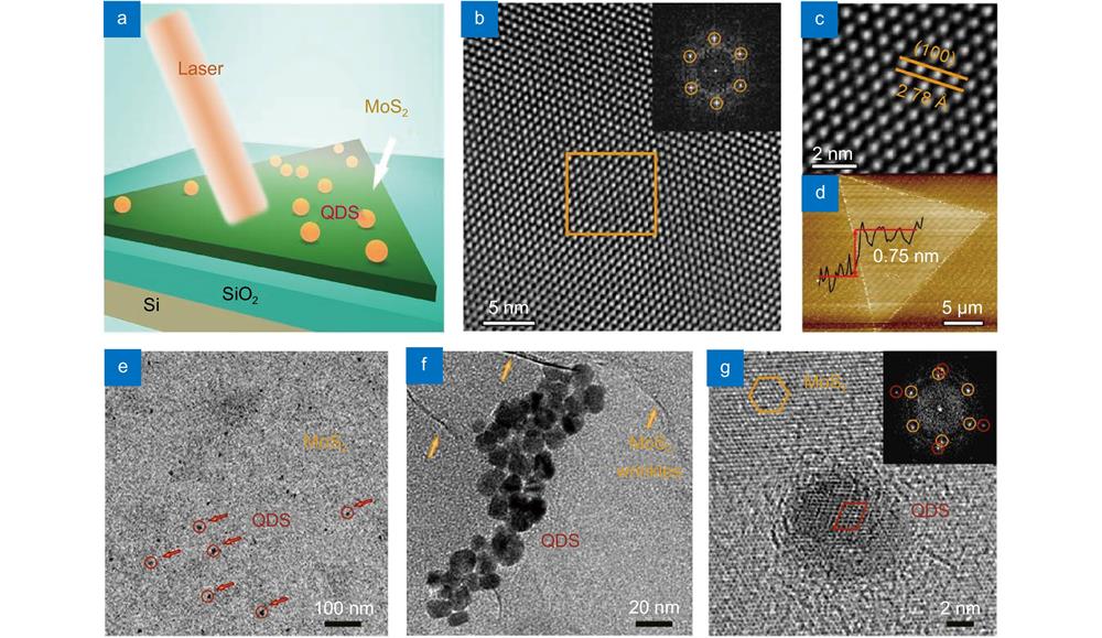
Figure 1(a) shows the schematic view of QD/MoS2 heterostructures under the excitation of a laser. MoS2 flakes were grown on SiO2/Si substrate in a chemical vapor deposition (CVD) process. To fabricate mixed-dimensional 0D/2D vdWHs, a drop of solution with 0.025 mg·L−1 CdSe/ZnS QDs was then dropped onto a prepared CVD-grown MoS2/SiO2/Si substrate. The density of QDs on substrates can be controlled by choosing the number of spin-coating times. From the optical images of pure MoS2 flakes and 0D/2D vdWHs (Supplementary information S1), it can be obviously observed that the optical contrast of MoS2 flakes varies when QDs are overlapped.
![]()
Figure 1.
The structure and morphology of as-prepared QD/MoS2 heterostructures can be confirmed by transmission electron microscopy (TEM) and atomic force microscopy (AFM). Figure 1(b) shows the high-resolution TEM image of MoS2 monolayer. Our MoS2 samples are of high-quality that there are no defects or substitute atoms observed from measurements. The inset shows the corresponding selected area electron diffraction (SAED) pattern. The pattern only presents one set of six-fold symmetry diffraction spots, which is stemming from the hexagonal atom arrangement of MoS2 flakes. The enlarged high-resolution TEM (HRTEM) image is shown in Fig. 1(c), which is derived from the marked squares in Fig. 1(b). The interplanar spacing is measured to be 2.78 Å corresponding to (100) planes of hexagonal MoS2. AFM topography of MoS2 monolayer shows a clear triangular shape, and the thickness is determined to be 7.5 Å (1 Å=10−10m).
After the wetting transfer process, QD/MoS2 heterostructures can be successfully transferred onto the Cu grid. Figure 1(e) shows the low-resolution TEM image of QD/MoS2 heterostructures, where QDs are randomly distributed on the surface of MoS2 monolayer, which have been marked by the red arrows. The scale bar is 100 nm. From a HRTEM image with the scale bar of 20 nm, the diameters of QDs are ranging from 8−15 nm (Fig. 1(f) and Supporting Information S2). Notably, the wrinkles or the edges of MoS2 monolayer are clearly observed as orange arrows point, which confirms that the as-transferred films are intact. From an enlarged area of HRTEM image of QD/MoS2 heterostructure (Fig. 1(g)), Moiré patterns can be observed at the edge of QDs, which is caused by overlapping lattices between MoS2 and QDs. The scale bar is 2 nm. The corresponding SAED image shows two different sets of arranged diffraction patterns, as shown in the inset of Fig. 1(g). The orange circles show a six-fold symmetry diffraction spots from MoS2, while the red circles exhibit a parallelogram configuration from CdSe/ZnS QDs.
The optical and spectral properties have been investigated among CdSe/ZnS QDs, MoS2 monolayers and their heterostructures. Figure 2(a) shows the UV-visible absorption spectrum of QDs solution, where two dominant absorption peaks are observed at around 450 nm and 620 nm. The PL spectra of QDs solution (0.2 mg·L−1) and QDs film on SiO2/Si substrate show Lorentzian lineshapes, where the peak center is 650 nm with a full width at half maximum (FWHM) of 45 nm. Although the excitation conditions are different, the PL spectrum of QDs on substrate exhibits a slightly-stronger spectral broadening than QDs in solutions. It is because of the change of the dielectric environment of exciton emissions.
![]()
Figure 2.
Figure 2(b) shows the Raman spectra of MoS2 monolayer (red curve) and QD/MoS2 heterostructures (purple curve). Two typical Raman peaks of MoS2 monolayer are observed at 384.2 cm−1 and 404.3 cm−1, which correspond to the E12g and A1g vibrational modes, respectively. The difference between these modes in the as-synthesized MoS2 monolayer is approximately 20.1 cm−1, which is slightly larger than the mechanically exfoliated monolayer MoS2 because of the crystalline strain
The absorption spectrum of MoS2 monolayer is measured as shown in Fig. 2(c), which is derived from the differential reflectance spectra between MoS2/substrate and substrate under white light illuminations. Two absorption peaks are observed to be located at approximately 622 nm and 659 nm, which correspond to direct excitonic transitions at K points in the Brillouin zone of MoS2. Correspondingly, the PL spectrum of MoS2 monolayer presents two featured peaks at 630 nm and 678 nm, respectively. In 0D/2D vdWHs, PL spectra show two peaks at 650 nm and 677 nm
PL intensity mapping has been performed to show spectral change in MoS2 monolayer and heterostructures. Figure 2(d) and 2(e) show the images of PL mapping of MoS2 monolayer at 665−750 nm and 640−660 nm, respectively, which are consistent with PL peaks of QDs and exciton A of MoS2. It is obviously observed that the PL intensity is dominant at the spectral range of exciton A. Images of PL intensity mapping of vdWHs are shown in Fig. 2(f) (665−750 nm) and Fig. 2(g) (640−660 nm). In comparison to Fig. 2(d), the PL intensity of heterostructure in Fig. 2(f) decreases a little owing to the interfacial charge transfer, and the intensity distribution shows slight inhomogeneity. While at the detection wavelength of 640−660 nm, the intensity of heterostructure is slightly stronger than that of MoS2 monolayer, where the intensity enhancement is mainly from the high-efficiency emission of QDs. Besides, a few QDs islands distributed on the substrate can also be observed. The laser powers are controlled at 0.3 mW for all the mapping measurements, and all the scale bars in Fig. 2(d−g) are 5 μm.
Time-resolved photoluminescence (TRPL) spectroscopy was carried out to further study and understand the spectral quenching caused by charge transfer. Fluorescence lifetime detection were obtained with 0.4 mg L−1 QD/MoS2 samples excited by a pulsed laser (400 nm, 80 MHz), at an excitation power of 0.3 mW. The signals were subsequently filtered by 650/50 nm bandpass filters, which can collect the full PL spectral range of QDs while keeping away from the main PL peak of MoS2 monolayer. The PL lifetimes for the two samples in Fig. 2(h) can be fitted and estimated using a biexponential decay model (
Figure 2(i) shows the energy band diagram of QD/MoS2 heterostructures. The conduction band and valence band of MoS2 monolayer are reported to be 4.25 eV and 6.1 eV in previous work, respectively
To estimate the charge doping efficiency in heterostructures at various concentrations, the analysis of spectral evolution are performed to demonstrate the contribution of both exciton and trion in the PL spectra. Figure 3(a) shows the competition between exciton and trion emissions when the QD concentration is increased. At low concentrations, the exciton components are dominated in the total spectra, while the weight of exciton decreases as the concentration increases. All the components are fitted using Lorenze line-shaped peaks (Supporting Information S4).
![]()
Figure 3.
The three-energy-levels model is shown in Fig. 3(b) to illustrate the competition between exciton and trion. Exciton is excited from the ground state to exciton energy level under the laser excitation (G). In an assumption that the trion is generated from the exciton in a non-radiative channel (Ktr(n)). Both the exciton (Γex = 0.002 ps−1) and trion (Γtr = 0.02 ps−1) in MoS2 monolayer generate PL signals in radiative channels. Then, the rate equations for the population of exciton (NA) and trion (NA’) can be expressed as
where Ktr (n) is the formation rate of trion that relates with the QDs concentration (n), and Ktr (0) = 0.5 ps−1 is the formation rate of trion for the pure MoS2 film
Figure 3(c) plots the changing trend of total PL intensity, exciton and trion at various concentrations. Both the total PL intensity and the exciton intensity attenuate greatly as the concentration increases. Because the charge transfer electrons become abundant with high QDs concentrations, the recombination process of electron-hole pairs is deeply suppressed. However, the intensity of trion is almost unchanged in the doping process, which is due to the Pauli blocking effect and many-body interactions that the luminescence of the trion is easily saturated at low doping levels
To further study the modulation ability of light-induced charge transfer and competitive exciton emissions, the laser-power dependent spectra of QDs, MoS2 and heterostructures with 0.025 mg L−1 QDs have been systematically investigated. Figure 4(a) and 4(b) show power-dependent PL spectra of MoS2 and QDs, respectively. When laser powers are increased from 65 to 670 μW, the intensity enhancement factors are determined as P=I/I0, where I and I0 are the intensities detected at high and low laser powers, respectively. P are detected as 8.4 for MoS2 exciton A and 7 for trion, respectively (Supporting Information S7). While for QDs, the intensity enhancement factor is detected as 20, and peak positions are stably appearing at 650 nm.
![]()
Figure 4.
Figure 4(c) shows the PL spectral evolution of QD/MoS2 heterostructures with increasing laser powers ranging from 65 to 670 μW. There is an obvious competition between QD exciton (green), MoS2 exciton A (blue) and trion (purple). At low power densities (<120 μW), MoS2 exciton and trion emissions are dominant resulting in a higher PL intensity larger than QDs. When laser powers are further increased, all components of exciton and trion get stronger, but the increasement speed behaves differently. It can be observed that the component of QDs exciton increases much fast, which gets stronger and becomes comparable to the component of MoS2 exciton at about 120 μW (Supporting Information S8).
The evolution of peak intensity of exciton and trion with laser powers has been plotted in Fig. 4(d). Both x-axis and y-axis are presented in log scales. The relationship of PL intensity (I) and laser power can be approximately written as I=(P)m, where m denotes exponent. For QD exciton, m decreases from 1.28 to 1.15 (QDs exciton in heterostructures). The value of m obtained from exciton A of MoS2 decreases from 0.9 to 0.87 (exciton A in heterostructures). The difference of PL sensitive-response gives rise to the competition and spectral evolution at various light powers. Figure 4(e) shows the schematics to illustrate the light-controlled spectral change. The blue rectangular and dotted orange rectangular show the areas of MoS2 flakes and QDs films, respectively. In a QD/MoS2 heterostructure with low QD density (as shown as the overlapping region), the number of MoS2 excitons excited at low laser powers is larger than QDs excitons. However, when the laser powers are increased to a high level, more QD excitons are generated, which are comparable to the contribution of MoS2 excitons, or even larger than that. The light-controlled spectral evolution shows the potential ability of tunable light-matter interactions in TMDs, which helps to influence the performance of optoelectronic devices.
The photo-induced charge behaviors are crucial to improve the performance of optoelectronic devices. The phototransistors of pristine MoS2 and vdWHs are systematically investigated, and their characteristics of photocurrents are measured to investigate the influence of interfacial charge doping. Figure 5(a) shows the schematic view of the device, where MoS2 monolayer served as a channel in the mix-dimensional FET (field-effect transistor), and Au/Cr (100 nm/5 nm) metal served as source/drain contacts on the back-gate Si/SiO2 substrate. Under the light illumination, electrons from QDs are transferred into MoS2 monolayer resulting in an efficient charge doping. The dilute solution of QDs can be uniformly spin-coated onto the MoS2 monolayer to realize the mixed-dimensional vdWHs device.
![]()
Figure 5.
To evaluate the optoelectronic performance of the vdWHs device compared to that of the MoS2 transistor, we investigated the photo-induced transfer curves (Fig. 5(b)), as well as the current–voltage characteristics in the dark and under illuminations (Fig. 5(c)). Both pristine MoS2 and hybrid phototransistors exhibit a typical n-type behavior in the dark. The threshold voltages of pristine MoS2 and heterostructure phototransistors are obtained as −20 V and −60 V. As shown from the photoinduced transfer curves (Ids−Vg) under the illumination (520 nm), Ids of the photodetector in the dark is increased by ~4.8 times compared to that of the pristine MoS2 device (7.55×10⁻⁷ A vs 1.56×10⁻⁷ A) at Vg=60 V. The enhanced drain currents (Ids) under the illumination are obtained as 4.4 times for pure MoS2 device (from 1.56×10⁻⁷ A to 6.86×10⁻⁷ A) and 11.3 times for QD/MoS2 heterostructure device (from 7.55×10⁻⁷ A to 8.52×10⁻⁶ A) at Vg=60 V, respectively. It can be understood that the strong light absorption of QDs and the effective charge separation at the interface contribute to the amplified photocurrents in vdWHs devices. Ids and Vg are the channel current and the gate voltage, respectively.
Furthermore, the photoresponsivity (R=Iph/Peff) and specific detectivity (D*=RS(1/2)/(2eId)1/2) are calculated to investigate the device performance, where Iph is the difference between photocurrent intensity and the dark-state current intensity, Peff is the effective incident laser power (Peff=Pin×Sdevice/Slaserspot), Sdevice is the effective detection area of the device, Id is the dark current, and e is the unit charge. Figure 5(d) and 5(e) show the calculated values of R and D* as a function of Peff, respectively, and the maximum values are detected at Vg = 60 V (the D* versus Vg is presented in the Supporting Information S11). The calculated R of the hybrid device is enhanced by 21.4 times (from 733 A·W–1 to 1.57×10⁴ A·W–1) compared to that of the pristine MoS2 device, which is an outstanding performance compared to that of other TMD-based photodetectors (Supporting Information S12). Furthermore, the calculated R value exponentially increases as the incident power decreases due to the reduced scattering and recombination. The obtained highest D* for the heterostructure device is enhanced by a factor of 9.6 compared to that of the pristine MoS2 photodetector (from 2.98×10¹⁰ Jones to 2.86×10¹¹ Jones).
We now discuss the possible mechanisms for improved photoresponsivities in these vdWHs devices. Both the photogating and photoconducting effects can coexist at the nanoscale interface, but the dominant mechanism varies. For the photoconductive effect, the current intensity linearly increases with excitation laser powers (I∝Peff), while it shows sublinear trend for photogating effect (I∝Peffα and α<1)
Finally, the photoswitching characteristics of the hybrid photodetector are investigated under pulsed illumination powers over multiple cycles at Vds = 1 V (Fig. 5(f)), and the rising time and the decay time extracted from the dynamic curves are shown in Fig. 5(g). Our mixed-dimensional photodetector exhibit stable and reproducible on-off photoswitching property, and the average rise and fall times are characterized to be 0.49 s and 0.6 s, respectively. Both the rise and fall curves in photocurrent can be fitted to a single exponential function. Figure 5(h) shows the Ids−Vg curves of heterostructure devices overlapped with various QDs concentrations, where the photocurrent intensities (Vds=1 V, Vg=0 V) increases as the concentration increases. It confirms that the enhancement of light absorption from QDs can generate more photoinduced carriers and improve the detection photoresponsivity of devices.
Conclusions
In summary, we have demonstrated that interfacial charge transfer in 0D/2D mixed-dimensional vdWHs can be tailored and utilized to enhance the optoelectronic performance of phototransistors. A series of morphology characteristics and spectral measurements, including high-resolution TEM, AFM, Raman shift, suppressed fluorescence intensity, and short PL lifetime provide strong evidences to show type-II band alignment induced charge transfer. In a model of three-energy-levels, an effect photo-induced doping can be estimated as 3.9×1013 cm−2, which contributes to the improved carrier mobility and enhanced optoelectronic performance of device in comparison with pure MoS2 device (1.57×10⁴ A·W−1 vs 733 A·W−1, 2.86×10¹⁰ Jones vs 2.98×10¹⁰ Jones @520 nm) at a low power density (≈0.1 nW). Furthermore, the detuning of laser power and back-gate voltage provides an alternative way to manipulate the gain mechanism of device. Therefore, the interfacial control of charge transfer gives more freedoms to optimize the optoelectronic features of mixed-dimensional vdWHs, which may bring more opportunities for the coming atomic-level device integrations.
References
[1] Z Zhang, P Lin, QL Liao, Z Kang, HN Si et al. Graphene-based mixed-dimensional van der Waals heterostructures for advanced optoelectronics. Adv Mater, 31, 1806411(2019).
[2] D Jariwala, TJ Marks, MC Hersam. Mixed-dimensional van der Waals heterostructures. Nat Mater, 16, 170-181(2017).
[3] QS Zeng, Z Liu. Novel optoelectronic devices: transition-metal-dichalcogenide-based 2D heterostructures. Adv Electron Mater, 4, 1700335(2018).
[4] C Hu, DD Dong, XK Yang, KK Qiao, D Yang et al. Synergistic effect of hybrid PbS quantum dots/2D-WSe2 toward high performance and broadband phototransistors. Adv Funct Mater, 27, 1603605(2017).
[5] XF Song, XH Liu, DJ Yu, CX Huo, JP Ji et al. Boosting two-dimensional MoS2/CsPbBr3 photodetectors via enhanced light absorbance and interfacial carrier separation. ACS Appl Mater Interfaces, 10, 2801-2809(2018).
[6] TF Yang, X Wang, BY Zheng, ZY Qi, C Ma et al. Ultrahigh-performance optoelectronics demonstrated in ultrathin perovskite-based vertical semiconductor heterostructures. ACS Nano, 13, 7996-8003(2019).
[7] F Li, YX Feng, ZW Li, C Ma, JY Qu et al. Rational kinetics control toward universal growth of 2D vertically stacked heterostructures. Adv Mater, 31, 1901351(2019).
[8] F Prins, AJ Goodman, WA Tisdale. Reduced dielectric screening and enhanced energy transfer in single- and few-layer MoS2. Nano Lett, 14, 6087-6091(2014).
[9] Z Lin, BR Carvalho, E Kahn, RT Lv, R Rao et al. Defect engineering of two-dimensional transition metal dichalcogenides. 2D Mater, 3, 22002(2016).
[10] S Bertolazzi, S Bonacchi, GJ Nan, A Pershin, D Beljonne et al. Engineering chemically active defects in monolayer MoS2 transistors via ion-beam irradiation and their healing via vapor deposition of alkanethiols. Adv Mater, 29, 1606760(2017).
[11] DA Nguyen, HM Oh, NT Duong, S Bang, SJ Yoon et al. Highly enhanced photoresponsivity of a monolayer WSe2 photodetector with nitrogen-doped graphene quantum dots. ACS Appl Mater Interfaces, 10, 10322-10329(2018).
[12] ZW Li, CX Liu, X Rong, Y Luo, HT Cheng et al. Tailoring MoS2 valley-polarized photoluminescence with super chiral near-field. Adv Mater, 30, 1801908(2018).
[13] ZW Li, Y Li, TY Han, XL Wang, Y Yu et al. Tailoring MoS2 exciton-plasmon interaction by optical spin-orbit coupling. ACS Nano, 11, 1165-1171(2017).
[14] HT Ying, X Li, HM Wang, YR Wang, X Hu et al. Band structure engineering in MoS2 based heterostructures toward high-performance phototransistors. Adv Opt Mater, 8, 2000430(2020).
[15] HL Hou, XW Zhang. Rational design of 1D/2D heterostructured photocatalyst for energy and environmental applications. Chem Eng J, 395, 125030(2020).
[16] G Konstantatos, M Badioli, L Gaudreau, J Osmond, M Bernechea et al. Hybrid graphene–quantum dot phototransistors with ultrahigh gain. Nat Nanotech, 7, 363-368(2012).
[17] DS Zheng, JL Wang, WD Hu, L Liao, HH Fang et al. When nanowires meet ultrahigh ferroelectric field−high-performance full-depleted nanowire photodetectors. Nano Lett, 16, 2548-2555(2016).
[18] WJ Luo, QC Weng, MS Long, P Wang, F Gong et al. Room-temperature single-photon detector based on single nanowire. Nano Lett, 18, 5439-5445(2018).
[19] D Kufer, T Lasanta, M Bernechea, FHL Koppens, G Konstantatos. Interface engineering in hybrid quantum dot–2D phototransistors. ACS Photonics, 3, 1324-1330(2016).
[20] AA Bessonov, M Allen, YL Liu, S Malik, J Bottomley et al. Compound quantum dot-perovskite optical absorbers on graphene enhancing short-wave infrared photodetection. ACS Nano, 11, 5547-5557(2017).
[21] CR Kagan, E Lifshitz, EH Sargent, DV Talapin. Building devices from colloidal quantum dots. Science, 353, aac5523(2016).
[22] HM Wang, CH Li, PF Fang, ZL Zhang, JZ Zhang. Synthesis, properties, and optoelectronic applications of two-dimensional MoS2 and MoS2-based heterostructures. Chem Soc Rev, 47, 6101-6127(2018).
[23] YPV Subbaiah, KJ Saji, A Tiwari. Atomically thin MoS2: a versatile nongraphene 2D material. Adv Funct Mater, 26, 2046-2069(2016).
[24] YC Cheng, HJW Li, B Liu, LY Jiang, M Liu et al. Vertical 0D-perovskite/2D-MoS2 van der Waals heterojunction phototransistor for emulating photoelectric-synergistically classical pavlovian conditioning and neural coding dynamics. Small, 16, 2005217(2020).
[25] HL Wu, Z Kang, ZH Zhang, Z Zhang, HN Si et al. Interfacial charge behavior modulation in perovskite quantum dot-monolayer MoS2 0D-2D mixed-dimensional van der Waals heterostructures. Adv Funct Mater, 28, 1802015(2018).
[26] HL Wu, HN Si, ZH Zhang, Z Kang, PW Wu et al. All-inorganic perovskite quantum dot-monolayer MoS2 mixed-dimensional van der Waals heterostructure for ultrasensitive photodetector. Adv Sci, 5, 1801219(2018).
[27] LW Zhang, SL Shen, M Li, LY Li, JB Zhang et al. Strategies for air-stable and tunable monolayer MoS2-based hybrid photodetectors with high performance by regulating the fully inorganic trihalide perovskite nanocrystals. Adv Opt Mater, 7, 1801744(2019).
[28] P Luo, FW Zhuge, FK Wang, LY Lian, KL Liu et al. PbSe quantum dots sensitized high-mobility Bi2O2Se nanosheets for high-performance and broadband photodetection beyond 2 μm. ACS Nano, 13, 9028-9037(2019).
[29] X Tang, KWC Lai. Graphene/HgTe quantum-dot photodetectors with gate-tunable infrared response. ACS Appl Nano Mater, 2, 6701-6706(2019).
[30] I Nikitskiy, S Goossens, D Kufer, T Lasanta, G Navickaite et al. Integrating an electrically active colloidal quantum dot photodiode with a graphene phototransistor. Nat Commun, 7, 11954(2016).
[31] H Liu, C Wang, T Wang, XM Hu, DM Liu et al. Controllable interlayer charge and energy transfer in perovskite quantum dots/transition metal dichalcogenide heterostructures. Adv Mater Interfaces, 6, 1901263(2019).
[32] SK Zhang, XD Wang, Y Chen, GJ Wu, YC Tang et al. Ultrasensitive hybrid MoS2-ZnCdSe quantum dot photodetectors with high gain. ACS Appl Mater Interfaces, 11, 23667-23672(2019).
[33] S Ahn, WJ Chen, MA Moreno-Gonzalez, M Lockett, JY Wang et al. Enhanced charge transfer and responsivity in hybrid quantum dot/graphene photodetectors using ZnO as intermediate electron-collecting layer. Adv Electron Mater, 6, 2000014(2020).
[34] GL Ye, YJ Gong, JH Lin, B Li, YM He et al. Defects engineered monolayer MoS2 for improved hydrogen evolution reaction. Nano Lett, 16, 1097-1103(2016).
[35] SS Li, YC Lin, W Zhao, J Wu, Z Wang et al. Vapor-liquid-solid growth of monolayer MoS2 nanoribbons. Nat Mater, 17, 535-542(2018).
[36] P Liu, XQ Zhu, C Feng, M Huang, J Li et al. Enhanced p-type behavior in the hybrid structure of graphene quantum dots/2D-WSe2. Appl Phys Lett, 111, 111603(2017).
[37] H Cho, SH Jeong, MH Park, YH Kim, C Wolf et al. Overcoming the electroluminescence efficiency limitations of perovskite light-emitting diodes. Science, 350, 1222-1225(2015).
[38] ZJ Ning, XW Gong, R Comin, G Walters, FJ Fan et al. Quantum-dot-in-perovskite solids. Nature, 523, 324-328(2015).
[39] IW Cho, MY Ryu. Enhancement of luminescence properties and stability in perovskite hybrid structure with CdSe/ZnS quantum dots. APL Mater, 7, 051112(2019).
[40] IW Cho, MY Ryu. Effect of energy transfer on the optical properties of surface-passivated perovskite films with CdSe/ZnS quantum dots. Sci Rep, 9, 18433(2019).
[41] JM Lanzafame, RJD Miller, AA Muenter, BA Parkinson. Ultrafast charge-transfer dynamics at tin disulfide surfaces. J Phys Chem, 96, 2820-2826(1992).
[42] HY Shi, RS Yan, S Bertolazzi, J Brivio, B Gao et al. Exciton dynamics in suspended monolayer and few-layer MoS2 2D crystals. ACS Nano, 7, 1072-1080(2013).
[43] B Liu, WJ Zhao, ZJ Ding, I Verzhbitskiy, LJ Li et al. Engineering bandgaps of monolayer MoS2 and WS2 on fluoropolymer substrates by electrostatically tuned many-body effects. Adv Mater, 28, 6457-6464(2016).
[44] KF Mak, KL He, C Lee, GH Lee, J Hone et al. Tightly bound trions in monolayer MoS2. Nat Mater, 12, 207-211(2013).
[45] J Suh, TE Park, DY Lin, DY Fu, J Park et al. Doping against the native propensity of MoS2: degenerate hole doping by cation substitution. Nano Lett, 14, 6976-6982(2014).
[46] JS Ross, SF Wu, HY Yu, NJ Ghimire, AM Jones et al. Electrical control of neutral and charged excitons in a monolayer semiconductor. Nat Commun, 4, 1474(2013).
[47] S Mouri, Y Miyauchi, K Matsuda. Tunable photoluminescence of monolayer MoS2 via chemical doping. Nano Lett, 13, 5944-5948(2013).
[48] L Li, WK Wang, Y Chai, HQ Li, ML Tian et al. Few-layered PtS2 phototransistor on h-BN with high gain. Adv Funct Mater, 27, 1701011(2017).
[49] OJ Island, SI Blanter, M Buscema, der van, A Castellanos-Gomez. Gate controlled photocurrent generation mechanisms in high-gain In2Se3 phototransistors. Nano Lett, 15, 7853-7858(2015).


Set citation alerts for the article
Please enter your email address

© Copyright 2018-2021 | Chinese Laser Press. All Rights Reserved 沪ICP备15018463号-20