
Quanxin Yang, Hongliang Liu, Shan He, Qingyu Tian, Bin Xu, Pengfei Wu. Circular cladding waveguides in Pr:YAG fabricated by femtosecond laser inscription: Raman, luminescence properties and guiding performance[J]. Opto-Electronic Advances, 2021, 4(2): 200005-1
- Opto-Electronic Advances
- Vol. 4, Issue 2, 200005-1 (2021)
Abstract
Introduction
In the past decades, femtosecond laser inscription (FLI) as a new method for micromachining
Praseodymium ions (Pr3+) present extremely complex energy level and relatively low photon energy, which make them applicable for laser transitions with different excitation wavelengths ranging from visible to infrared. During the past few years, laser generations have been reported based on different Pr-doped fluoride materials: waveguide laser in Pr:YLF
In this paper, we exhibit the fabrication of circular cladding waveguides with low propagation losses in Pr:YAG crystal by using FLI. By investigating the guiding mode profiles and confocal μ-Raman properties, localized modification effects caused by the femtosecond laser and the guiding mechanism are revealed. In addition, luminescence and guiding properties of the guiding area are also studied.
Method
Waveguide fabrication
The Pr:YAG crystal sample (praseodymium doped yttrium aluminum garnet, Pr:Y3Al5O12, doped by 0.5 at. % Pr3+ ions, obtained from Atom Optics Co. Ltd, Shanghai, China) used in this work is cut into dimensions of 10 mm × 6 mm × 2 mm with all facets optically polished. During the waveguide fabrication process, an amplified Ti:sapphire laser system (Astrella, Coherent Inc., USA) is used as laser source, which generates linearly polarized pulses (with repetition rate of 1 kHz, central wavelength of 800 nm, pulse width of 35 fs, and single pulse energy of 7 mJ). Watt Pilot motorized attenuator and a neutral density filter are utilized to adjust the laser power precisely, and specifically, single pulse energy of 0.23 μJ is used in this work. The laser beam is focused by a microscope objective (40 ×, NA = 0.6) into the substrate beneath a 10 mm × 6 mm facet (the upper facet). The substrate is placed on a 6-axes precision motorized stage and the scanning speed is set to be 0.8 mm/s.
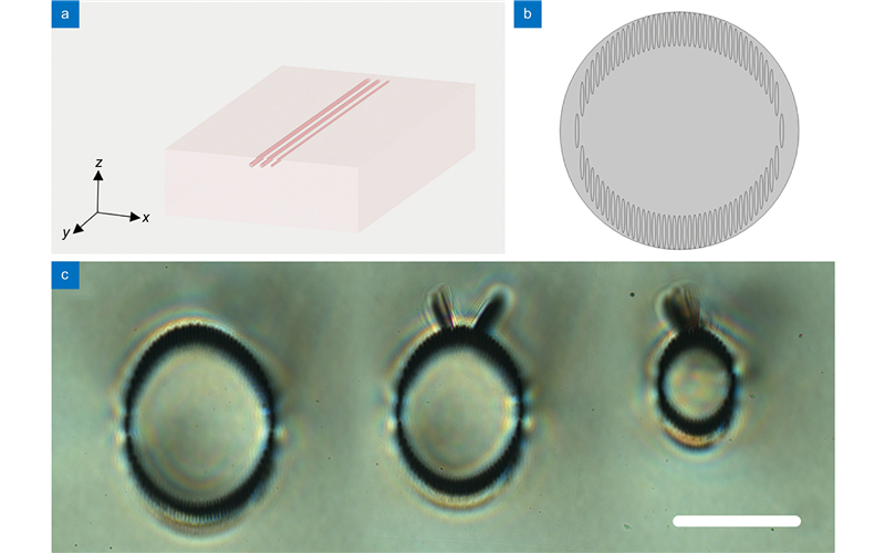
Under the above experiment conditions, one damage track with vertical width of 15 μm and horizontal width of 2.6 μm can be inscribed via a single scan. Arrays of parallel damage tracks are inscribed following the designed geometries (the horizontal separation between adjacent tracks is 3 μm) so as to form desired cladding waveguides with different diameters, as shown in Fig. 1. All the waveguides are fabricated along the y-axis of the substrate (i.e., the waveguide lengths are all 10 mm).
![]()
Figure 1.(
Confocal μ-Raman measurement and luminescence characterization
Raman properties of the femtosecond laser induced damage tracks and the formed guiding core area are explored by a confocal μ-Raman spectroscopy system (XperRam200, Nanobase, South Korea). A continuous laser beam (532 nm, 30 mW) is focused onto the end-face by a microscope objective (40 ×, NA = 0.75). Part of the beam is affected by the Raman scattering effect of the sample and is then collected and transferred to a spectrometer system. With the help of a galvo scanning system, we can accurately gain the Raman properties of every region over the whole waveguide cross-section.
As for the luminescence characterization experiment process, a continuous laser beam at 400 nm is focused onto the end-face of the sample. And the emergent light from another end-face is collected and transferred to a spectrometer system which can provide the luminescence information of irradiated area in real time.
Waveguide characterization and guiding mode simulation
The near field intensity distributions of guiding modes are measured by an end-face coupling system. This system uses a 632.8 nm He-Ne laser as light source. A Glan-Taylor prism and a 1/2 waveplate at 632.8 nm are utilized to generate linear-polarized incident laser beam (i.e. TE and TM, TE: the electric field is parallel to the x-axis; TM: parallel to the z-axis). The linearly polarized beam is then coupled into one waveguide by a microscope objective (40 ×, NA = 0.65) and the transmission light is collected by a long working distance microscope objective (50 ×, NA = 0.55) from another end-face. The profile is subsequently imaged via a CCD camera (WCD-UCD12-1310, DataRay, USA).
The guiding mode simulation process is accomplished by the finite element method (FEM). The geometry structures used for simulation, as shown in Fig. 1(b), are determined by referring to the micrographs and 2D μ-Raman mapping images, as shown in Fig. 1(c) and Fig. 3, respectively. Since the mechanical stress produced by the physical lattice expansion at damage tracks attenuates rapidly over distance and has negligible influence on the waveguide core area, and to simplify the refractive index distribution used in the simulation, we assume a step-index configuration with the refractive index difference of -0.04 at all damage track boundaries.
Results and discussion
Figures 1(a) and 1(b) exhibit the 3D and 2D geometry structures of waveguides, and the 2D one is also used in the guiding mode simulation process. Figure 1(c) shows the cross-section microscope images (optical transmission) of the circular cladding waveguides with different diameters: 120 μm, 100 μm, and 60 μm, respectively. Since our aim of this work is to build waveguides that fit the demand of luminescence and laser generation, we are making waveguides with relatively large diameters. But according to our former experience, cladding waveguides with minimum diameter of 10 μm can be fabricated in such kind of crystal. The damage tracks (of different fabricated waveguides) closest to the upper facet share a depth of 120 μm beneath the upper facet. The refractive index change in the track regions is estimated to be -0.04 by measuring the NA value of the waveguides. No evident damage in the core areas of the fabricated waveguides is oberserved.
Raman properties of one fabricated waveguide with diameter of 120 μm are shown in Fig. 2 and Fig. 3. Raman spectra accurately measured at different positions reveal the variation of lattice after FLI process. As we can see from Fig. 2, the Raman intensity at damage track region suffers a strong quenching without evident variation on the spectral distribution while the Raman spectra of non-processed bulk area and waveguide volume are indistinguishable.
In order to further investigate the Raman spectra variation over the whole waveguide cross-section, the 2D mapping is implemented and the corresponding results are presented in Fig. 3. Intensity, shift and full width at half maximum (FWHM) changes of characteristic peak (259 cm-1) are shown as different channels. And significant differences: Raman intensity quenching, blue shift (i.e., wavenumber decrease) and broadening of the emission peak can be observed at the damage track regions. These phenomena indicate the formation of lattice defects/damages and the elongation of bond-lengths (i.e., lattice parameter) due to the expansive stress. The partial dilatation also results in the refractive index decrease at these regions. Therefore, the refractive index induced guiding mechanism of such cladding waveguides can be ascertained. Otherwise, the waveguide volume manifests fairly similar Raman properties with respect to the non-processed bulk area, which demonstrates that the lattice structure in the guiding area is well preserved during the FLI process.
![]()
Figure 2.
A further analysis about the Raman spectra of damage tracks and the surrounding areas is introduced here. As mentioned above, significant differences are observed at the damage tracks with respect to the non-processed bulk area. Raman intensity quenching and peak broadening originates from the formation of lattice defects and damages; while for peak blue shift, the elongation of bond-lengths becomes the dominant factor. That is in good agreement with the subjective impressions, which is longer bond-lengths correspond to lower molecular vibration frequencies, closer molecular vibration energy levels, and lower Raman shift for specific peaks. But when we focus on the surrounding areas of damage tracks, a strong red shift (i.e., wavenumber increase) occurs without evident variation on Raman intensity or FWHM with respect to the non-processed bulk area, indicating a homogeneous lattice compression at these areas. In other words, regions modified by the femtosecond laser present lattice dilatation with refractive index decrease while the surrounding areas are squeezed by the modified regions, forming lattice compression with refractive index increase. This phenomenon is in agreement with several published works accomplished on different samples
![]()
Figure 3.
Figure 4 depicts the luminescence emission spectra of the guiding volume of one fabricated 120 μm waveguide and non-processed bulk area. Virtually identical emission spectra (both spectral distribution and intensity) indicate that the luminescence properties of Pr3+ ions at waveguide volume have been well preserved during the FLI process.
All the fabricated cladding waveguides support both TE and TM polarizations (following the aforesaid definition). Since the diameters of the fabricated waveguide are relatively large (~100 μm) compared to the incident laser wavelength (632.8 nm), large amounts of high-order modes are supported to propagate in the waveguides. Because of that, different modes with different intensity distributions and effective refractive indexes can be excited when the incident laser beam is focused on different relative positions with respect to the waveguide volume.
![]()
Figure 4.
The guiding modes with a specific kind of intensity distribution of waveguides with different diameters and the corresponding simulation results are exhibited in Fig. 5. These guiding modes possess horizontal fringes with TE polarization, which is actually the characteristic of LP1n modes (LP mode: linearly polarized mode). It's worth mentioning that these modes only exist when the incident laser beam is focused on the positions a little bit right above or below the waveguide center. As can be seen in this figure, the experiment and the simulation results match well.
![]()
Figure 5.
Here, we introduce a further discussion about the origin of guiding modes with this specific kind of intensity distributions. In consideration of the similarity between the observed modes and the typical modes in optical fiber, an ideal step-index circularly-symmetric fiber model that has the same refractive index profile and waveguide core area with the 60 μm cladding waveguide model is established. Simulation result indicates that such fiber supports the propagation of TE04 mode, as shown in Fig. 6(a). Circularly symmetric fiber supports the propagation of modes with the same electric field distribution but different poloidal rotation angles about the fiber axis, and these modes present nearly indistinguishable effective refractive indexes, which means, they are degenerate. In addition, simulation method that we used (using effective refractive indexes to distinguish modes, mode analysis, FEM) tends to show a combined mode as result instead of several degenerate modes if they have nearly the same effective refractive indexes. Based on the above points, gained TE04 mode can be separated into two orthogonally polarized LP14 modes. The obtained LP14 modes present the same electric field distribution with a poloidal rotation of 90°, and Fig. 6(c) shows the LP14 mode with horizontal polarization. It should be noticed that, generally, a specific LP mode is viewed as a combination of several vector modes including TE, TM, EH, and HE because LP mode is gained using weakly guiding approximation. But since LP mode can be expressed by vector modes, vice versa, a specific vector mode can be expressed by several LP modes.
![]()
Figure 6.
Since these LP14 modes are degenerate, they are more inclined to combine and form a circularly symmetric TE04 mode in simulation, which means, a single LP14 mode will not emerge under such condition. But if under non-circularly-symmetric condition, such as in elliptical fiber, previous degenerate modes with different polarizations will manifest similar electric-field distributions and slightly different effective refractive indexes, scilicet the removal of degeneracy
The losses of the waveguides at 632.8 nm when the incident laser is differently polarized are given in Table 1. The total losses are directly measured by an optical power meter and the end-face coupling system used in the measurement of the intensity distributions of guiding modes while the coupling losses are roughly calculated by the BeamPROP module of Rsoft Photonics CAD Suite. The main simulation parameters are listed here: spot diameter of 10 μm; refractive index difference of -0.04. Therefore, the propagation losses of the waveguides can be directly given and the error induced during the measurements should be less than ±0.2 dB/cm. Since the beam diameter of 10 μm is relatively small compared to the waveguide diameters of 100 and 120 μm, simulation results reveal the same coupling loss value of the waveguides with diameters of 100 and 120 μm. The propagation losses result shows such circular cladding waveguides in Pr:YAG present fairly low propagation losses at 632.8 nm.
| 60 μm | 100 μm | 120 μm | ||
| Total loss (dB) | TE | 3.60 | 3.31 | 3.46 |
| TM | 4.06 | 3.70 | 3.86 | |
| Coupling loss (dB) | TE/TM | 3.47 | 3.16 | 3.16 |
| Propagation loss (dB/cm) | TE | 0.13 | 0.15 | 0.3 |
| TM | 0.59 | 0.54 | 0.7 |
Table 1.
Conclusions
In conclusion, we have successfully fabricated circular cladding waveguides which support multi-mode propagation with orthogonal polarizations in Pr:YAG crystal by FLI. The fabricated waveguides show good guiding performance without any deterioration of the luminescence properties of the Pr3+ ions in the waveguide volume. A specific kind of guiding mode profiles is analyzed in detail, and simulation results suggest the feasibility of mode profile control in such waveguides. By means of the Raman property analysis of damage tracks and the surrounding areas, we have ascertained the modification effects of femtosecond laser and the refractive index induced guiding mechanism. With excellent luminescence performance and fairly low propagation losses, the fabricated waveguides present potential for integrated luminescence and laser generation applied in advances photonics circuits.
References
[1] D Zhang, K Sugioka. Hierarchical microstructures with high spatial frequency laser induced periodic surface structures possessing different orientations created by femtosecond laser ablation of silicon in liquids. Opto-Electron Adv, 2, 190002(2019).
[2] X Liu, B Bai, Q Chen, H Sun. Etching-assisted femtosecond laser modification of hard materials. Opto-Electron Adv, 2, 190021(2019).
[3] LM Zhang, TY Guo, YY Ren, YJ Cai, MD Mackenzie et al. Cooperative up-converted luminescence in Yb, Na:CaF2 cladding waveguides by femtosecond laser inscription. Opt Commun, 441, 8-13(2019).
[4] V Bharadwaj, A Courvoisier, TT Fernandez, R Ramponi, G Galzerano et al. Femtosecond laser inscription of Bragg grating waveguides in bulk diamond. Opt Lett, 42, 3451-3453(2017).
[5] B Sotillo, V Bharadwaj, JP Hadden, M Sakakura, A Chiappini et al. Diamond photonics platform enabled by femtosecond laser writing. Sci Rep, 6, 35566(2016).
[6] SL Li, FM Deng, ZP Huang. Femtosecond laser inscription waveguides in Nd:GdVO4 crystal. Opt Eng, 55, 107104(2016).
[7] H Chandrahalim, SC Rand, XD Fan. Fusion of renewable ring resonator lasers and ultrafast laser inscribed photonic waveguides. Sci Rep, 6, 32668(2016).
[8] MR Vázquez, B Sotillo, S Rampini, V Bharadwaj, B Gholipour et al. Femtosecond laser inscription of nonlinear photonic circuits in Gallium Lanthanum Sulphide glass. J Phys Photonics, 1, 015006(2018).
[9] SL Li, YK Ye, CY Shen, HL Wang. Femtosecond laser inscribed cladding waveguide structures in LiNbO3 crystal for beam splitters. Opt Eng, 57, 117103(2018).
[10] T Piromjitpong, M Dubov, S Boscolo. High-repetition-rate femtosecond-laser inscription of low-loss thermally stable waveguides in lithium niobate. Appl Phys A, 125, 302(2019).
[11] JM Lv, YZ Cheng, QM Lu, de Vázquez, XT Hao et al. Femtosecond laser written optical waveguides in z-cut MgO:LiNbO3 crystal: Fabrication and optical damage investigation. Opt Mater, 57, 169-173(2016).
[12] F Chen, de Vázquez. Optical waveguides in crystalline dielectric materials produced by femtosecond-laser micromachining. Laser Photonics Rev, 8, 251-275(2014).
[13] Y Jia, S Wang, F Chen. Femtosecond laser direct writing of flexibly configured waveguide geometries in optical crystals: fabrication and application. Opto-Electron Adv, 3, 190042(2020).
[14] N Skryabin, A Kalinkin, I Dyakonov, S Kulik. Femtosecond laser written depressed-cladding waveguide 2 × 2, 1 × 2 and 3 × 3 directional couplers in Tm(3+):YAG crystal. Micromachines (Basel), 11, 1(2019).
[15] YY Ren, Y Jiao, de Vázquez, F Chen. Ti:Sapphire micro-structures by femtosecond laser inscription: Guiding and luminescence properties. Opt Mater, 58, 61-66(2016).
[16] JP Bérubé, J Lapointe, A Dupont, M Bernier, R Vallée. Femtosecond laser inscription of depressed cladding single-mode mid-infrared waveguides in sapphire. Opt Lett, 44, 37-40(2019).
[17] SL Li, ZP Huang, YK Ye, HL Wang. Femtosecond laser inscribed cladding waveguide lasers in Nd:LiYF4 crystals. Opt Laser Technol, 102, 247-253(2018).
[18] C Romero, Ajates García, F Chen, de Vázquez. Fabrication of tapered circular depressed-cladding waveguides in Nd:YAG crystal by femtosecond-laser direct inscription. Micromachines (Basel), 11, 10(2019).
[19] WJ Nie, RY He, C Cheng, U Rocha, de Vázquez et al. Optical lattice-like cladding waveguides by direct laser writing: fabrication, luminescence, and lasing. Opt Lett, 41, 2169-2172(2016).
[20] HL Liu, SY Luo, B Xu, HY Xu, ZP Cai et al. Femtosecond-laser micromachined Pr:YLF depressed cladding waveguide: Raman, fluorescence, and laser performance. Opt Mater Express, 7, 3990-3997(2017).
[21] AG Okhrimchuk, LN Butvina, EM Dianov, NV Lichkova, VN Zagorodnev et al. New laser transition in a Pr3+:RbPb2Cl5crystal in the 2.3—2.5-μm range. Quantum Electron, 36, 41-44(2006).
[22] HK Nie, PX Zhang, BT Zhang, KJ Yang, LH Zhang et al. Diode-end-pumped Ho, Pr:LiLuF4 bulk laser at 2.95 μm. Opt Lett, 42, 699-702(2017).
[23] MQ Fan, T Li, GQ Li, SZ Zhao, KJ Yang et al. Passively Q-switched Ho, Pr:LiLuF4 laser with graphitic carbon nitride nanosheet film. Opt Express, 25, 12796-12803(2017).
[24] YJ Cheng, J Peng, B Xu, H Yang, ZQ Luo et al. Passive Q-switching of a diode-pumped Pr:LiYF4 visible laser using WS2 as saturable absorber. IEEE Photonics J, 8, 1-6(2016).
[25] M Fibrich, J Šulc, A Zavadilová, H Jelínková. Nonlinear mirror mode-locked Pr:YAlO3 laser. Laser Phys, 27, 055801(2017).
[26] S Sattayaporn, P Loiseau, G Aka, DT Marzahl, C Kränkel. Crystal growth, spectroscopy and laser performances of Pr(3+):Sr0.7La0.3Mg0.3Al11.7O19 (Pr:ASL). Opt Express, 26, 1278-1289(2018).
[27] PF Wu, S He, HL Liu. Annular waveguide lasers at 1064 nm in Nd:YAG crystal produced by femtosecond laser inscription. Appl Opt, 57, 5420-5424(2018).
[28] HL Liu, de Vázquez, MH Hong, F Chen. Femtosecond laser inscribed Y-branch waveguide in Nd:YAG crystal: Fabrication and continuous-wave lasing. IEEE J Sel Top Quantum Electron, 22, 227-230(2016).
[29] S McDaniel, F Thorburn, A Lancaster, R Stites, G Cook et al. Operation of Ho:YAG ultrafast laser inscribed waveguide lasers. Appl Opt, 56, 3251-3256(2017).
[30] MH Kim, T Calmano, SY Choi, BJ Lee, IH Baek et al. Monolayer graphene coated Yb:YAG channel waveguides for
[31] I Gómez-Castellanos, RM Rodriguez-Dagnino. Intensity distributions and cutoff frequencies of linearly polarized modes for a step-index elliptical optical fiber. Opt Eng, 46, 045003(2007).
Acknowledgements
Author contributions
Competing interests


Set citation alerts for the article
Please enter your email address

© Copyright 2018-2021 | Chinese Laser Press. All Rights Reserved 沪ICP备15018463号-20