Journals >Journal of Infrared and Millimeter Waves
Contents


2022
Volume: 41 Issue 6
20 Article(s)
Export citation format
Research Articles
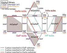
The magic of III-Vs
Yong-Gang ZHANG, Yi GU, Ying-Jie MA, Xiu-Mei SHAO, Xue LI, Hai-Mei GONG, and Jia-Xiong FANG
III-V compound semiconductors have abundant features for various electronic, optoelectronic and photonic applications, all arise from variform magic combination of group III and group V elements formed binaries, resulting in ever-changing characteristics. In this paper, diversified ternaries, quaternaries and quinariesIII-V compound semiconductors have abundant features for various electronic, optoelectronic and photonic applications, all arise from variform magic combination of group III and group V elements formed binaries, resulting in ever-changing characteristics. In this paper, diversified ternaries, quaternaries and quinaries are presented geometrically based on the binaries of arsenide, phosphide and antimonide, mainly concerned of their bandgap, lattice constant and the lattice match domain on different substrates. The features of nitride and dilute nitride, bismide and dilute bismuth, as well as boride, are also discussed briefly. An overall observation of whole III-Vs may contribute to the comprehensive understanding of their latent capacity and sustainable development, along with a lot of challenges..
Journal of Infrared and Millimeter Waves
- Publication Date: Dec. 25, 2022
- Vol. 41, Issue 6, 941 (2022)


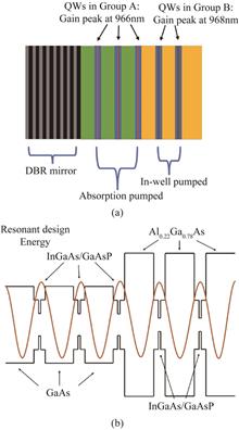
Quantum well modulated optical pumped vertical external cavity surface-emitting laser for dual-wavelength generation
Zhi-Wei LI, Zhuo ZHANG, Jian-Wei ZHANG, Xing ZHANG, Yin-Li ZHOU, Yu-Gang ZENG, Yong-Qiang Ning, and Li-Jun WANG
Optically pumped dual-wavelength vertical external cavity surface-emitting semiconductor laser (VECSEL) with a single gain chip is reported. The active region of the gain chip is composed of two groups of quantum wells with different lasing wavelengths, one group of quantum wells with shorter wavelength operates by absOptically pumped dual-wavelength vertical external cavity surface-emitting semiconductor laser (VECSEL) with a single gain chip is reported. The active region of the gain chip is composed of two groups of quantum wells with different lasing wavelengths, one group of quantum wells with shorter wavelength operates by absorption pumping, and the other group of quantum wells with longer wavelength operates by in-well pumping. When the VECSEL is operating, the short-wavelength quantum wells pumped by the absorption region are first lased, due to the intensity modulation effect of the long-wavelength quantum wells on the short-wavelength quantum wells, it can be observed that the peak intensity of the spectrum oscillates periodically with time, pulsed operation of the VECSEL was observed by the highly sensitive detector. With the increasing of the pump power, stable dual-wavelength emission was achieved, the peak positions of emission wavelength are 967.5 nm and 969.8 nm respectively. The output power of the stable dual-wavelength emission can reach 560 mW, and the far fields show Gaussian cross-sections in orthogonal dimensions, and the divergence angles of 6.68° and 6.87° are obtained..
Journal of Infrared and Millimeter Waves
- Publication Date: Dec. 25, 2022
- Vol. 41, Issue 6, 951 (2022)
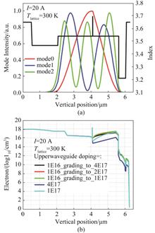
Design considerations to increase the power-efficiency of a supper-large-optical-cavity waveguide structure diode laser
Kun ZHOU, Lin-An HE, Yi LI, Yu-Wen HE, Wei-Chuan DU, Sheng-Zhe LIU, Liang ZHANG, Yao HU, Liang SONG, Song-Xin GAO, and Chun TANG
The considerations in the epitaxial and longitudinal design of a supper-large-optical-cavity structure diode laser in the 976-nm band are numerically studied and presented here. Mode control layers were designed underneath and up the quantum well layer to suppress the lasing of high-order transverse modes. The electronThe considerations in the epitaxial and longitudinal design of a supper-large-optical-cavity structure diode laser in the 976-nm band are numerically studied and presented here. Mode control layers were designed underneath and up the quantum well layer to suppress the lasing of high-order transverse modes. The electron leakage was suppressed by a band energy engineering, where the electron barrier increases from the p-waveguide layer to the p-cladding layer. The optimized structure has an internal loss of 0.66 cm-1, an internal quantum efficiency of 0.954, and a full width at half maximum vertical far-field angle of 17.4°. For the resonant cavity design, a liner current profile along the cavity was proposed to reduce the longitudinal spatial hole burning effect, where a power penalty of 1.0 W at 20 A is suppressed. The 4-mm-long and 100 μm wide broad-area single emitter with the supper-large-optical-cavity epitaxial structure was designed to have a high power-efficiency of about 71% at an output power of 21 W under continuous current injection at 25°C..
Journal of Infrared and Millimeter Waves
- Publication Date: Dec. 25, 2022
- Vol. 41, Issue 6, 958 (2022)
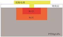
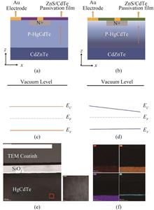
Study on HgCdTe APD focal plane technology
Xiong-Jun LI, Ying-Xu ZHANG, Xiao CHEN, Li-Hua LI, Peng ZHAO, Zhen-Yu YANG, Dong YANG, Wei-bo JIANG, Peng-wei YANG, Jin-Cheng KONG, Jun ZHAO, and Rong-Bin JI
A 256×256 HgCdTe APD hybrid focal plane array (FPA) with 30μm pixel pitch was prepared by B ion implantation n-on-p planar junction technology based on MW HgCdTe material grown by LPE. The performance parameters such as gain, dark current and noise factor were characterized and analyzed at liquid nitrogen temperatA 256×256 HgCdTe APD hybrid focal plane array (FPA) with 30μm pixel pitch was prepared by B ion implantation n-on-p planar junction technology based on MW HgCdTe material grown by LPE. The performance parameters such as gain, dark current and noise factor were characterized and analyzed at liquid nitrogen temperature. The results show that the average gain of HgCdTe APD focal plane chip is 166.8 and the gain non-uniformity is 3.33% under - 8.5V reverse bias; Under 0 ~ - 8.5V reverse bias, the gain normalized dark current of APD device is 9.0×10⁻¹⁴A~1.6×10⁻¹³A, the noise factor F is between 1.0 and 1.5. In addition, the imaging demonstration of HgCdTe APD focal plane is carried out, and a good imaging effect is obtained..
Journal of Infrared and Millimeter Waves
- Publication Date: Dec. 25, 2022
- Vol. 41, Issue 6, 965 (2022)
High speed uncooled MWIR infrared HgCdTe photodetector based on graded bandgap structure
Mao-Sheng SANG, Guo-Qing XU, Hui QIAO, and Xiang-Yang LI
A high-speed room-temperature mid-wave infrared HgCdTe photodetector based on graded bandgap structure was reported. This study explores a n-on-p homojunction structure on epitaxial HgCdTe, which achieves a total response time of 1.33 ns (750 MHz) under zero bias voltage at 300 K, which is faster than commercial uncoolA high-speed room-temperature mid-wave infrared HgCdTe photodetector based on graded bandgap structure was reported. This study explores a n-on-p homojunction structure on epitaxial HgCdTe, which achieves a total response time of 1.33 ns (750 MHz) under zero bias voltage at 300 K, which is faster than commercial uncooled MCT photovoltaic photodetectors and MWIR HgCdTe APDs under high reverse bias. The analysis based on one-dimensional equations shows that compositional grading in the absorber layer can form built-in electric field and the transport mechanism of carriers is changed, the model is confirmed by the comparisons of different graded HgCdTe photodetectors. Thereby, this work facilitates design of the high-speed HgCdTe MWIR detectors, and provides a promising method to optimize the ultrafast MWIR infrared photodetectors..
Journal of Infrared and Millimeter Waves
- Publication Date: Dec. 25, 2022
- Vol. 41, Issue 6, 972 (2022)

Photoconductive focal plane arrays infrared detector based on PbSe
Yan-Song CHEN, Zi-Yang REN, Han-Lun XU, Hai-Ming ZHU, Yao WANG, and Hui-Zhen WU
The influence of the parameters of PbSe photoconductive infrared detector on the photoelectric response was simulated by the continuity equation of semiconductor non-equilibrium carriers. A small-scale pixel x-y addressable PbSe photoconductive focal plane array (FPA) detector was developed experimentally. The pixel siThe influence of the parameters of PbSe photoconductive infrared detector on the photoelectric response was simulated by the continuity equation of semiconductor non-equilibrium carriers. A small-scale pixel x-y addressable PbSe photoconductive focal plane array (FPA) detector was developed experimentally. The pixel size was 500 μm×500 μm, and the pixel pitch was 500 μm. The photoelectric response performance of the pixels of the PbSe FPA detector was experimentally characterized, and the effective pixel rate reached 100%. Under 500 K temperature blackbody radiation and 3.0 V bias voltage, the average responsivity and detectivity reached 110 mA/W and 5.5×10⁹ cmHz1/2W-1, respectively. The noise equivalent temperature difference (NETD) of the pixels ranged from 15 to 81 mK, and the average noise equivalent temperature difference was 32mK. Using a mid-wavelength infrared imaging device, the infrared thermal imaging of the PbSe FPA detector on the thermal radiation target of 350~450℃ was preliminarily demonstrated. This work lays the foundation for the subsequent development of high-density pixel PbSe FPA detectors..
Journal of Infrared and Millimeter Waves
- Publication Date: Dec. 25, 2022
- Vol. 41, Issue 6, 980 (2022)
Study on Molecular Beam Epitaxy of High indium InGaAs Films
Ying YANG, Hong-Zhen WANG, Liu-Yan FAN, Ping-Ping CHEN, Bo-Wen LIU, Xun-Jun HE, Yi GU, Ying-Jie MA, Tao LI, Xiu-Mei SHAO, and Xue LI
The effects of molecular beam epitaxy growth parameters on the properties of high indium InGaAs materials have been investigated in this paper. The growth temperature, V/III ratio and arsenic dimer of In0.74Ga0.26As materials were investigated and adjusted to optimize the peak intensity of the photo luminescence and X-The effects of molecular beam epitaxy growth parameters on the properties of high indium InGaAs materials have been investigated in this paper. The growth temperature, V/III ratio and arsenic dimer of In0.74Ga0.26As materials were investigated and adjusted to optimize the peak intensity of the photo luminescence and X-ray diffraction measurements, as well as background carrier concentration and mobility. Results show that moderate growth temperatures and V/III ratios are needed for the growth to improve the lattice quality, reduce the non-radiation recombination and decrease the background impurity concentration. The In0.74Ga0.26As materials grown using As2 dimer show better material quality than those using As4 dimer. For the material grown at 570 ℃, As2 dimer and V/III ratio of 18, relatively strong photo luminescence and X-ray diffraction peak intensity have been achieved. At room temperature and 77 K, the background carrier concentrations were 6.3×1014 cm-3 and 4.0×1014 cm-3, while the mobilities were 13 400 cm2/Vs and 45 160 cm2/Vs, respectively..
Journal of Infrared and Millimeter Waves
- Publication Date: Dec. 25, 2022
- Vol. 41, Issue 6, 987 (2022)
Growth and characterization of InAsP/InAsSb superlattices by Metal Organic Chemical Vapor Deposition for mid-wavelength detection
Yun-Long HUAI, Hong ZHU, He ZHU, Jia-Feng LIU, Meng LI, Zhen LIU, and Yong HUANG
“Ga-free” strain-balanced InAsP/InAsSb superlattices grown on InAs substrate by Metal Organic Chemical Vapor Deposition(MOCVD)was proposed and implemented to explore its feasibility as an infrared absorption material. First, the band gaps of InAsP/InAsSb superlattices were calculated by k·p method, and it was foun“Ga-free” strain-balanced InAsP/InAsSb superlattices grown on InAs substrate by Metal Organic Chemical Vapor Deposition(MOCVD)was proposed and implemented to explore its feasibility as an infrared absorption material. First, the band gaps of InAsP/InAsSb superlattices were calculated by k·p method, and it was found that their cut-off wavelength cover mid-wavelength infrared to long wave infrared region. Then, InAs0.8P0.2/InAs0.7Sb0.3 superlattices were chosen and grown on InAs substrate by MOCVD. XRD measurement shows that the lattice mismatches between the InAs substrate peak and 0th order satellite peak of superlattices is only 61", indicating strain balance condition is achieved. AFM test for surface morphology shows its root mean square roughness is only 0.4 nm for 5×5 μm2 regions. The low-temperature PL spectra shows strong superlattice emission with peak located around 3.3 μm, which is closed to the design value. All the results indicate the feasibility and practicality of strain balanced InAsP/InAsSb superlattices grown by MOCVD for infrared detection..
Journal of Infrared and Millimeter Waves
- Publication Date: Dec. 25, 2022
- Vol. 41, Issue 6, 995 (2022)
Performance test method of InGaAs near infrared detector for astronomical observation
Bai-Cheng SUN, Jie GUO, Fang-Yu XU, Ming-Guo FAN, Xiao-Xia GONG, Yong-Sheng XIANG, Yun LING, and Yu-Chen ZHANG
Based on the evaluation system of astronomical infrared detectors, the performance of two InGaAs NIR detectors, liquid nitrogen-cooled and thermoelectric-cooled, was tested using a modified "photon transfer curve" tests method. The measured value is 83 e-, which is much higher than the nominal value of 15 e-;Based on the evaluation system of astronomical infrared detectors, the performance of two InGaAs NIR detectors, liquid nitrogen-cooled and thermoelectric-cooled, was tested using a modified "photon transfer curve" tests method. The measured value is 83 e-, which is much higher than the nominal value of 15 e-; the high and low conversion factors of NIRvana are 1.25 ADU/e- and 0.097 ADU/e-, respectively, and the readout noise is 105 e- and 380 e-; the measured value of dark current of NIRvana at the high conversion factor step is 415 e-/s, which is about twice of the nominal value. The theoretical estimate of the signal electron number of the Yunnan Observatory two-meter ring telescope at 1.565 μm solar magnetic field measurement is about 8800 e-, and the NIRvana-LN detector signal-to-noise ratio is 70 under the measured dark current of 4.06 e-/s, image exposure time of 20 ms, and readout noise of 83.59 e-..
Journal of Infrared and Millimeter Waves
- Publication Date: Dec. 25, 2022
- Vol. 41, Issue 6, 1002 (2022)
Failure modes and analysis for HgCdTe linear photoconductive detectors
Hui QIAO, Ni-Li WANG, Tian-Yi LAN, Shui-Ping ZHAO, Qi-Zhi TIAN, Ye LU, Reng WANG, Qin HUO, Fan SHI, Yi-Dan TANG, Kai-Hui CHU, Jia JIA, Qing ZHOU, Xiao-Yu SUN, Pei-Lu JIANG, Yi LUO, Xin-Yi CHENG, and Xiang-Yang LI
Failure modes during screening tests and application processes have been summed up for HgCdTe linear photoconductive detectors which have been applied in several programs. The mechanisms behand these failure modes have been analyzed based on the combination of HgCdTe material parameters, device structure dimensions, deFailure modes during screening tests and application processes have been summed up for HgCdTe linear photoconductive detectors which have been applied in several programs. The mechanisms behand these failure modes have been analyzed based on the combination of HgCdTe material parameters, device structure dimensions, detector physics, fabrication processes and device test techniques. Criteria of failure modes have been firstly proposed for deeper understanding of HgCdTe linear photoconductive detector and better optimization of detector screening process, which are also helpful for the analysis and resolution of problems encountered in the application of HgCdTe linear photoconductive detectors..
Journal of Infrared and Millimeter Waves
- Publication Date: Dec. 25, 2022
- Vol. 41, Issue 6, 1009 (2022)
Regulation on microstructural and optical properties of Sb2Te3 films induced by titanium doping
Yuan-Jie LIAO, Yao-Peng LI, Xiao-Xiao SONG, Xin-Tong ZHANG, Shu-Bo ZHANG, Teng-Fei ZHANG, Meng-Qi LUY, Zhen LIU, Yi-Yun ZOU, Ye ZHANG, Er-Tao HU, and Jing LI
In this work, the doping effects of Ti on the structural, linear optical properties and nonlinear absorption of Sb2Te3 thin films were systematically studied. A magnetron sputtering system and an annealing furnace are employed to prepare the crystalline Sb2Te3 samples with different doping concentrations of Ti. The X-rIn this work, the doping effects of Ti on the structural, linear optical properties and nonlinear absorption of Sb2Te3 thin films were systematically studied. A magnetron sputtering system and an annealing furnace are employed to prepare the crystalline Sb2Te3 samples with different doping concentrations of Ti. The X-ray photoelectron spectroscopy analysis confirmed that the Ti element exists in the Sb2Te3 films is in the form of TiTe2, in which the chemical state of Ti4+ arises. For linear optical properties, the results indicate that the Ti dopant can improve the transmittance of the Sb2Te3 films, when a wide working wavelength is used in the nonlinear devices. The optical band gap decreases from 1.32 eV to 1.25 eV for the Ti-doped Sb2Te3 films, which is dependent on the reduction of carriers according to the Burstein-Moss theory. An open-aperture Z-scan system is set up to determine the nonlinear saturated absorption of the film samples, which is excited by an 800 nm femtosecond laser at a power of 132 GW/cm2. Moreover, the adjustable behavior caused by Ti doping could be attributed to the competition between the decrease in the optical band gap and the inhibition of the crystallization. Additionally, it is interesting to ?nd that the Ti doping improves the laser damage threshold of the Sb2Te3 thin films from 188.6 to 265.5 GW/cm2. In general, the Ti-doped Sb2Te3 thin films have wide-ranging application possibilities for the field of nonlinear optical devices..
Journal of Infrared and Millimeter Waves
- Publication Date: Dec. 25, 2022
- Vol. 41, Issue 6, 1022 (2022)
Design of high-frequency circuit for W-band CW sheet beam extended-interaction klystron
Qi JIN, Zhi-Hui GENG, Jian ZHANG, Rui ZHANG, Xiu-Dong YANG, Yun-Feng LIAO, and Shou-Xi XU
To solve the problem that W-band klystron is difficult to achieve CW (continuous wave) high power, we propose a W-band CW sheet beam extended-interaction klystron (EIK) high frequency circuit operating at TM31-2π mode. A sheet electron beam with a voltage of 20 kV, a current of 0.65 A and the dimension of 2.5 mm×0To solve the problem that W-band klystron is difficult to achieve CW (continuous wave) high power, we propose a W-band CW sheet beam extended-interaction klystron (EIK) high frequency circuit operating at TM31-2π mode. A sheet electron beam with a voltage of 20 kV, a current of 0.65 A and the dimension of 2.5 mm×0.3 mm is used. The high frequency system adopts five dumbbell type five-gap cavities and the output system adopts symmetrical output waveguide. By optimizing high-frequency structural parameters, the simulation results of 3D PIC show that more than 1200 W power can be obtained at an input power of 0.2 W, and the electron efficiency and gain are 9.35% and 37.8 dB respectively. In terms of sensitivity and error stability of high-frequency parameters, TM31 mode and TM11 mode are compared and analyzed in detail..
Journal of Infrared and Millimeter Waves
- Publication Date: Dec. 25, 2022
- Vol. 41, Issue 6, 1030 (2022)
Design of 220 GHz power amplifier based on 90 nm InP HEMT process
Yan CHEN, Fan-Zhong MENG, Yuan FANG, Ao ZHANG, and Jian-Jun GAO
Based on the 90 nm InP HEMT process, a 220 GHz power amplifier terahertz integrated circuit design (TMIC) is designed. The amplifier adopts the on-chip Wilkinson power divider structure to realize the power synthesis of two-way five stage common-source amplifiers. The on-wafer measurement results show that the average Based on the 90 nm InP HEMT process, a 220 GHz power amplifier terahertz integrated circuit design (TMIC) is designed. The amplifier adopts the on-chip Wilkinson power divider structure to realize the power synthesis of two-way five stage common-source amplifiers. The on-wafer measurement results show that the average small signal gain of the power amplifier is 18 dB. The power test results show that the saturated output power of the power amplifier is better than 15.8 mW from 210 GHz to 230 GHz, with a maximum output power of 20.9 mW at 223 GHz. The size of the TMIC chip is 2.18 mm×2.40 mm..
Journal of Infrared and Millimeter Waves
- Publication Date: Dec. 25, 2022
- Vol. 41, Issue 6, 1037 (2022)
Theoretical study and PIC simulation of a 220 GHz Gyro-TWT with periodic dielectric loaded waveguide
Ru-Tai CHEN, and Sheng YU
In this article, a 220 GHz gyro-TWT operating at fundamental harmonic TE01 mode with periodic dielectric loaded (PDL) waveguide was designed through theoretical study and particle in cell (PIC) simulation. The parasitic oscillations (absolute instability oscillation and backward wave oscillation) have been successfullyIn this article, a 220 GHz gyro-TWT operating at fundamental harmonic TE01 mode with periodic dielectric loaded (PDL) waveguide was designed through theoretical study and particle in cell (PIC) simulation. The parasitic oscillations (absolute instability oscillation and backward wave oscillation) have been successfully suppressed by study of start-up thresholds and loading dielectric rings. The beam wave interaction behaviors are compared between nonlinear theory programs and PIC simulation, the results are basically consistent. In PIC simulation, the optimized gyro-TWT was developed with saturated output power of 55.61 kW, corresponding efficiency of 26.48% at 220 GHz with 70 kV and 3A electron beam, the saturated gain is 53.56 dB, and -3dB bandwidth is 12 GHz..
Journal of Infrared and Millimeter Waves
- Publication Date: Dec. 25, 2022
- Vol. 41, Issue 6, 1042 (2022)
A waveform matching-based method of improving laser footprint geolocation for GaoFen-7 spaceborne laser altimeter in mountainous areas
Yu WU, Heng WANG, Qi-Jin HAN, Xiao-Xiang LONG, Yue MA, Qing-Peng LI, Pu-Fan ZHAO, and Song LI
This paper proposed a geolocation method for laser footprints based on the waveform matching. Specifically, for a single laser footprint, the simulated waveform based on airborne lidar point cloud data as prior measurements was matched with the captured waveform of the Gaofen-7 SLA. Within a laser track, the correlatioThis paper proposed a geolocation method for laser footprints based on the waveform matching. Specifically, for a single laser footprint, the simulated waveform based on airborne lidar point cloud data as prior measurements was matched with the captured waveform of the Gaofen-7 SLA. Within a laser track, the correlation coefficient of the matching results in successive footprints was calculated to further estimate the laser pointing and ranging information and re-geolocate the laser footprints in mountainous areas. A study area (the Utah State in USA) with local airborne lidar data was selected to verify the proposed method. With the mean surface slope of approximately 20°, the elevation accuracy of GaoFen-7’s laser footprints were improved from (2.45±2.93) m to (0.27±0.61) m, which proved the effectiveness of the proposed method..
Journal of Infrared and Millimeter Waves
- Publication Date: Dec. 25, 2022
- Vol. 41, Issue 6, 1051 (2022)
Calibration method of relative linear deviation angle of polarization three-dimensional imager
Yue ZHANG, Xue-Min ZHANG, Yi LIU, Xuan LI, Su ZHANG, Yue YU, Jian-Chao JIAO, and Yun SU
Based on introduction about principle of polarization three-dimensional image and components of four apertures polarization three-dimensional imager, the influence of four apertures relative polarization direction on polarization three-dimensional imaging accuracy was analyzed, to determine the accuracy requirements foBased on introduction about principle of polarization three-dimensional image and components of four apertures polarization three-dimensional imager, the influence of four apertures relative polarization direction on polarization three-dimensional imaging accuracy was analyzed, to determine the accuracy requirements for four apertures relative polarization directions. The calibration method of relative polarization direction of four linear polarizers in four aperture lenses and calibration method of relative polarization direction of four apertures polarization three-dimensional imager was developed. The calibration device was built, and the relative polarization direction calibration was carried out in the laboratory. The calibration error of relative polarization directions of four linear polarizers in four aperture lenses was ±0.5o. The calibration error of relative polarization direction of four apertures polarization three-dimensional imager was ±1o. Thus, the normal direction error of three-dimensional polarization inversion can be guaranteed to be -5.47%~5.80%,that would ensure high-quality imaging of four apertures polarization three-dimensional imager..
Journal of Infrared and Millimeter Waves
- Publication Date: Dec. 25, 2022
- Vol. 41, Issue 6, 1062 (2022)
Research on imaging model of infrared camera with focal plane detector and its MTF measuring method
Jian KONG, Yu-Tian FU, and Yue-Jin ZHAO
Imaging Model in space domain and frequency domain of an infrared camera with focal plane detector is established. It shows that because of the existence of back ground radiance and non-uniformity the geometrical performance of an infrared camera can be evaluated by MTF only when the camera is well-corrected and the liImaging Model in space domain and frequency domain of an infrared camera with focal plane detector is established. It shows that because of the existence of back ground radiance and non-uniformity the geometrical performance of an infrared camera can be evaluated by MTF only when the camera is well-corrected and the linearity and space invariance condition is satisfied. An MTF measurement method of an infrared camera using focal plane detector is given. This method does not depend on the well correction of the camera and can avoid the deviation from the background radiance..
Journal of Infrared and Millimeter Waves
- Publication Date: Dec. 25, 2022
- Vol. 41, Issue 6, 1072 (2022)
Optimum designs of micro-resonator photonic crystal waveguides with gradually varied formations
Li-Heng WU, and Ming-Hong WANG
In order to design high quality single pass-band wavelength channels, three types of micro-resonator photonic crystal waveguides with gradually varied formations are designed. Power transmission spectra of these waveguides are studied by using FDTD (Finite-Difference Time-Domain) method. The output performances of thesIn order to design high quality single pass-band wavelength channels, three types of micro-resonator photonic crystal waveguides with gradually varied formations are designed. Power transmission spectra of these waveguides are studied by using FDTD (Finite-Difference Time-Domain) method. The output performances of these structures are compared and analyzed by collecting the pass-bands parameters of power spectra. As the central rod radius value of the micro-resonator increases, single pass-band transmission patterns of every waveguide output show the law of three times regular periodic variations from the short wavelength to the long wavelength. Optimization of structural choices and structural parameter designs have favourable effects on the output performances, so all of these waveguides have promising potentials to develop more single pass-band wavelength channels. The results show that the optimized structures can possess high quality of single pass-band wavelength transmission characteristics, such as regular periodic variation patterns, favorable signal enhancement designs, stable transmission performances, excellent adaptability of broad bandwidth. The best type of the structural designs can be flexibly selected according to the required wavelength, and these waveguides have application values in the designs of dense optical communication system, integrated optical path, compact optical sensing interface etc..
Journal of Infrared and Millimeter Waves
- Publication Date: Dec. 25, 2022
- Vol. 41, Issue 6, 1081 (2022)
GPNet:Lightweight infrared image target detection algorithm
Xian-Guo LI, Ming-Teng CAO, Bin LI, Yi LIU, and Chang-Yun MIAO
A lightweight infrared image target detection algorithm GPNet is proposed to address the need for accurate and real-time target detection in resource-constrained infrared imaging systems. The feature extraction network is optimized using GhostNet, feature fusion is performed using an improved PANet, and a depth-separabA lightweight infrared image target detection algorithm GPNet is proposed to address the need for accurate and real-time target detection in resource-constrained infrared imaging systems. The feature extraction network is optimized using GhostNet, feature fusion is performed using an improved PANet, and a depth-separable convolution is used to replace the ordinary 3×3 convolution at specific locations to better extract multi-scale features and reduce the number of parameters. Experiments on public datasets show that the algorithm in this paper reduces the number of parameters by 81% and 42% compared with YOLOv4 and YOLOv5-m, respectively; the average mean accuracy is improved by 2.5% and the number of parameters is reduced by 51% compared with YOLOX-m; the number of parameters is 12.3 M and the detection time is 14 ms, which achieves a balance between detection accuracy and number of parameters..
Journal of Infrared and Millimeter Waves
- Publication Date: Dec. 25, 2022
- Vol. 41, Issue 6, 1092 (2022)
Light-weight infrared small target detection combining cross-scale feature fusion with bottleneck attention module
Zai-Ping LIN, Bo-Yang LI, Miao LI, Long-Guang WANG, Tian-Hao WU, Yi-Hang LUO, Chao XIAO, Ruo-Jing LI, and Wei An
This paper proposed a light-weight single frame infrared small target detection network that combined cross-scale feature fusion and bottleneck attention module. Instead of bringing extra huge neurons, the network directly performs cross-scale feature interaction between the encoding and decoding sub-networks, maintainThis paper proposed a light-weight single frame infrared small target detection network that combined cross-scale feature fusion and bottleneck attention module. Instead of bringing extra huge neurons, the network directly performs cross-scale feature interaction between the encoding and decoding sub-networks, maintain the response of small target in the deep CNN layers, and thus achieves the full fusion between the spatial structure features from shallow layers and high-level semantic features from deep layers. Based on cross-scale feature fusion module, a light-weight bottleneck attention module is introduced to further enhance the response the target feature in the deep layers of the network. Experimental results demonstrate that the network can effectively suppress the complex background clutter and achieve high performance of infrared small target detection with low amount of parameters..
Journal of Infrared and Millimeter Waves
- Publication Date: Dec. 25, 2022
- Vol. 41, Issue 6, 1102 (2022)

© Copyright 2018-2021 | Chinese Laser Press. All Rights Reserved 沪ICP备15018463号-20