
Lin Cheng, Kui Tang, Wang-Hung Ki, Feng Su. Fast-transient techniques for high-frequency DC–DC converters[J]. Journal of Semiconductors, 2020, 41(11): 112402
- Journal of Semiconductors
- Vol. 41, Issue 11, 112402 (2020)
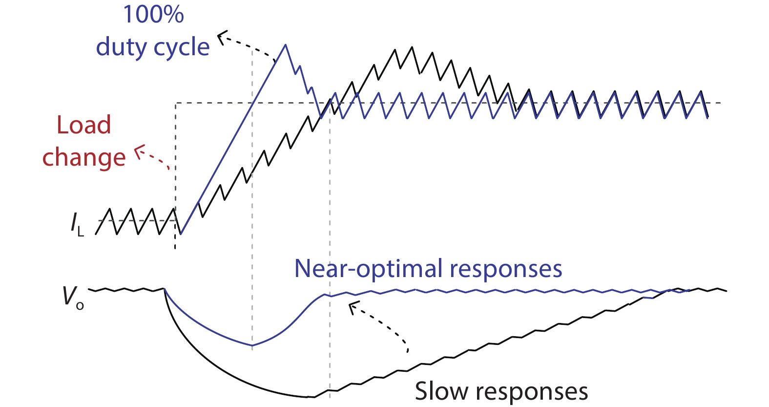
Fig. 1. (Color online) Transient-enhanced techniques for PWM control.
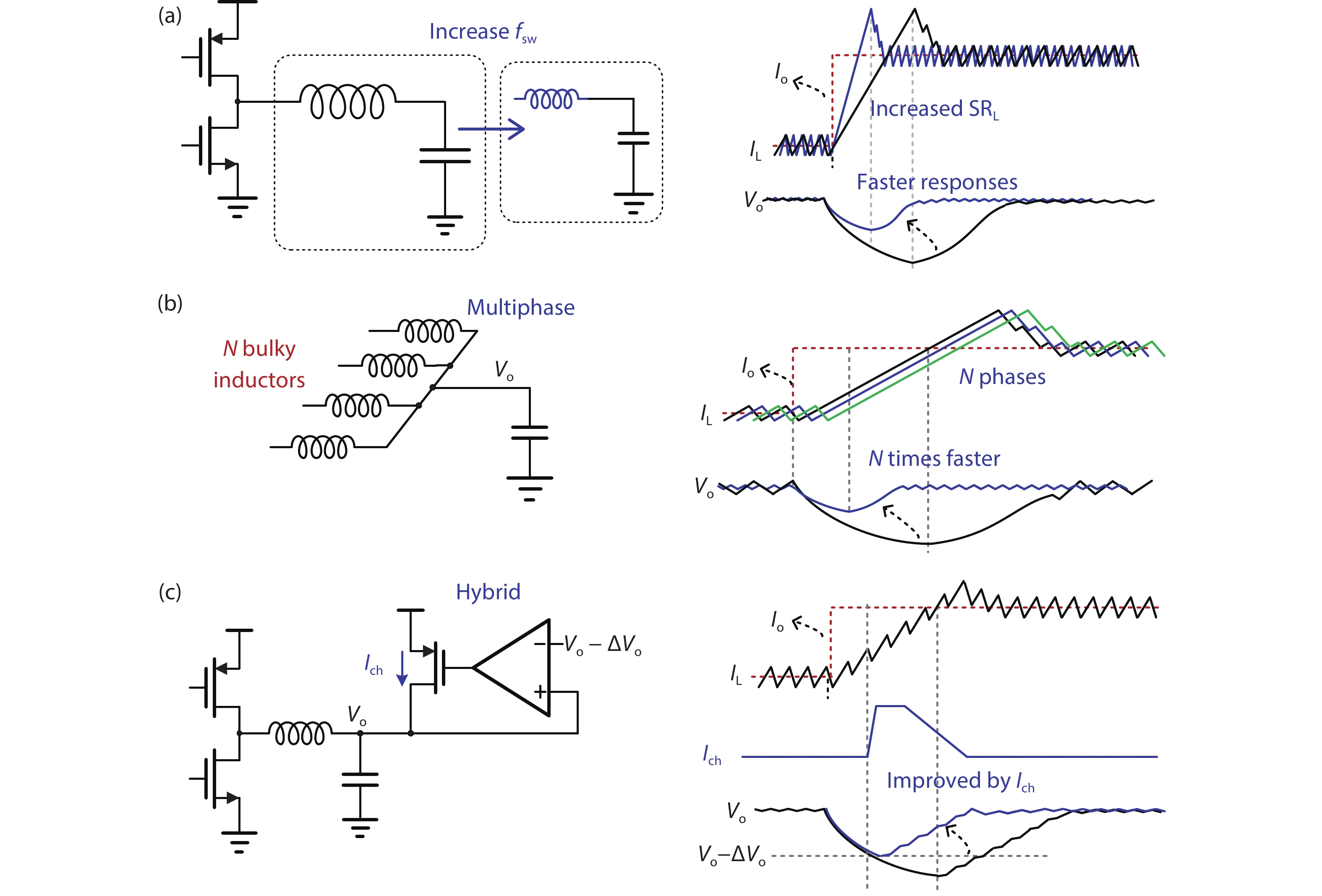
Fig. 2. (Color online) Techniques to overcome the limitation of slew rate of the inductor current (SRL): (a) increasing switching frequency, (b) multiphase topology, (c) hybrid scheme.
Fig. 3. Block diagram of the proposed buck converter.
Fig. 4. (a) Previous DDA-based Type-III compensator. (b) Possible improvement on the previous compensator. (c) New DDA-based Type-III compensator.
Fig. 5. Schematic of differential difference amplifier (DDA).
Fig. 6. Simulated frequency responses of (a) the two DDA-based Type-III compensators, (b) the loop-gain functions of the converters with the two compensators, and (c) the transfer functions from V fb to V Gm of the two compensators.
Fig. 7. Simulated transient responses. (a) Up-transient. (b) Down-transient.
Fig. 8. Simulated frequency responses with PVT variations: (a) proposed Type-III compensator, and (b) loop gain function.
Fig. 9. Simulated transient responses of the proposed converter. (a) Up transient. (b) Down-transient.
Fig. 10. Schematic of the accurate ramp generator.
Fig. 11. (Color online) The proposed hybrid scheme: (a) simplified schematic, (b) working principle.
Fig. 12. (Color online) Transient responses of the proposed converter (a) with PWM control only, (b) with the hybrid scheme.
Fig. 13. The detailed implementation of undershoot reduction branch circuit.
Fig. 14. (Color online) Simulated waveforms of the proposed hybrid scheme during an up transient.
Fig. 15. (Color online) Simulated transient responses of the proposed hybrid scheme.
Fig. 16. (Color online) Chip micrograph.
Fig. 17. (Color online) Measured steady-state waveforms when (a) I o = 1 A (CCM), (b) I o = 24 mA (DCM).
Fig. 18. (Color online) Measured power conversion efficiencies at different V o.
Fig. 19. (Color online) Measured load-transient responses of the converter.
Fig. 20. (Color online) Measured load-transient responses of the converter with and without the proposed hybrid scheme.
| ||||||||||||||||||||||||||||||||||||||||||||||||||||||||||||||||||||||||||||||||||||||||||||||||||||||||||||||||||||||||||||||||
Table 1. Performance comparison with previously published works.

Set citation alerts for the article
Please enter your email address
© Copyright 2018-2021 | Chinese Laser Press. All Rights Reserved 沪ICP备15018463号-20