
Lin Cheng, Kui Tang, Wang-Hung Ki, Feng Su. Fast-transient techniques for high-frequency DC–DC converters[J]. Journal of Semiconductors, 2020, 41(11): 112402
- Journal of Semiconductors
- Vol. 41, Issue 11, 112402 (2020)
Abstract
1. Introduction
With the growing demands for high performance computations, both the current consumption and the current slew rate of modern microprocessors have dramatically increased[
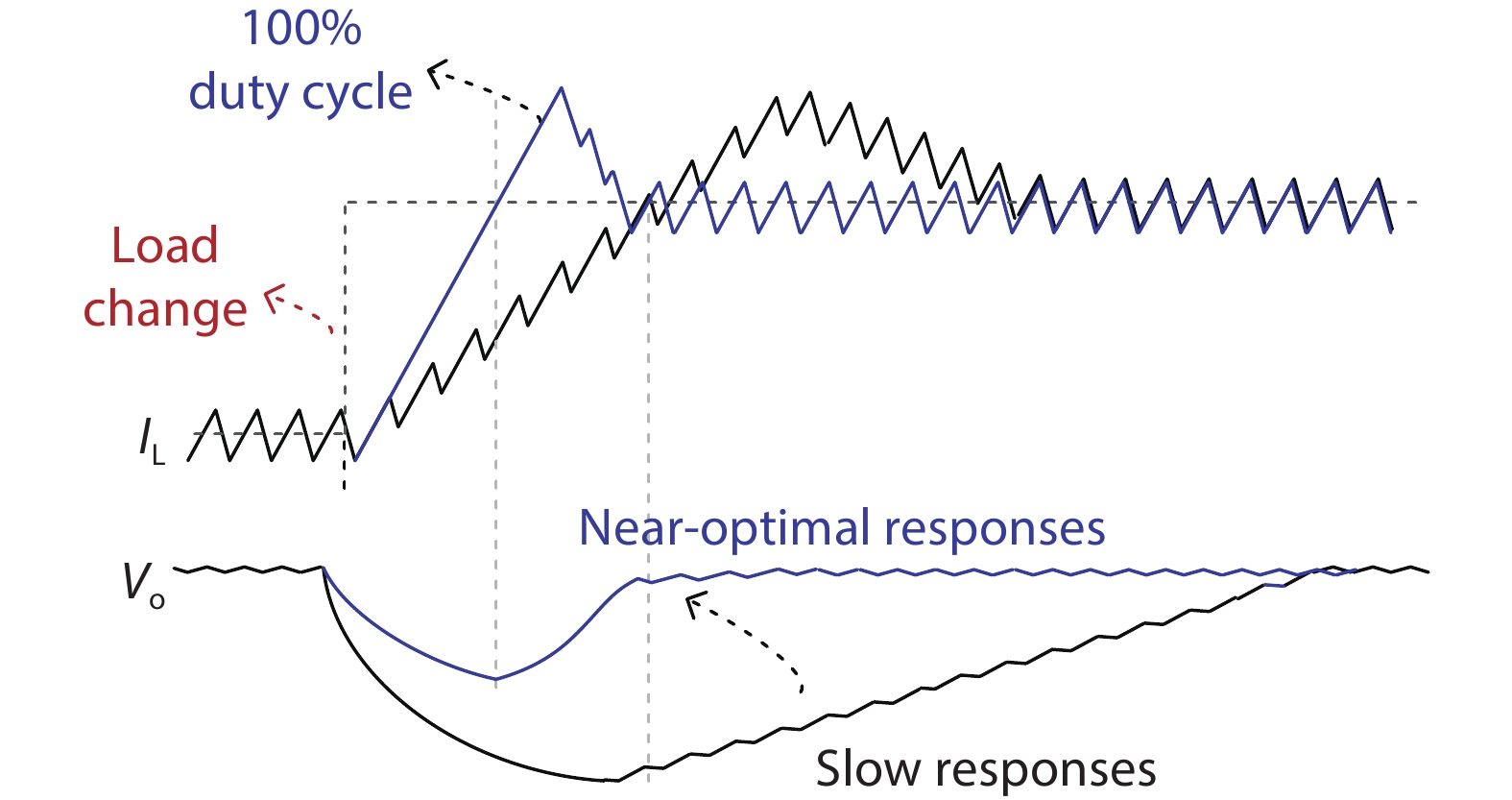
PWM control with fixed switching frequency has been attractive for its predictable noise spectrum and tight voltage regulation. However, it is usually believed that PWM control suffers from slow responses due to its limited loop bandwidth. Many fast-transient techniques have thus been proposed. During load transients, the slew rate of the error amplifier is increased in Refs. [5, 6], the ramp amplitude is adjusted in Ref. [7], V2 control is employed in Refs. [8–11], V1 concept is introduced in Ref. [12] and a capacitor-current-sensor (CCS) calibration technique with transient optimization is proposed in Ref. [13]. As shown in Fig. 1, the goals of these techniques are actually the same, and they are to enhance the speed of the PWM loop so that the inductor current (IL) ramps up (down) quickly to reduce the undershoot (overshoot) of the output voltage (Vo) and thus the settling times. On the other hand, to reduce the range of voltage fluctuation during load transients, adaptive voltage positioning (AVP) technique is proposed by designing the output impedance of the converter to be resistive[
![]()
Figure 1.(Color online) Transient-enhanced techniques for PWM control.
Compared to PWM control, hysteretic control is a more popular scheme for applications that require fast transient responses[
Using the above mentioned techniques, near-optimal transient responses may be achieved, but the response speed is still limited by the slew rate of the inductor current (SRL). Fig. 2 shows three approaches that can overcome this limitation. As shown in Fig. 2(a), one straightforward way is to use a smaller inductor and switch the converter at a higher frequency[
![]()
Figure 2.(Color online) Techniques to overcome the limitation of slew rate of the inductor current (SRL): (a) increasing switching frequency, (b) multiphase topology, (c) hybrid scheme.
In this paper, a 30 MHz voltage-mode controlled buck converter with fast transient responses is presented[
![]()
Figure 3.Block diagram of the proposed buck converter.
2. Design of improved DDA-based Type-III compensator
2.1. Improved DDA-based Type-III compensator
As shown in Fig. 4(a), a DDA-based Type-III compensator is proposed to save silicon area in Ref. [23], but one additional DC bias for Vcom is needed and the differential input range of the DDA has to be sufficiently large for proper operation. Although fast reference-tracking responses can be achieved with the help of the end-point prediction scheme, it suffers from long settling times during load transients, which are due to the slow responses at VGm. Fig. 5 shows the implementation of the DDA: a folded-cascode amplifier with two differential input pairs[
![]()
Figure 4.(a) Previous DDA-based Type-III compensator. (b) Possible improvement on the previous compensator. (c) New DDA-based Type-III compensator.
![]()
Figure 5.Schematic of differential difference amplifier (DDA).
Therefore, Vfb (= V2–) is equal to V2+ in the steady state. It means that the transconductance amplifier (OTA) that is used to regulate Vfb to be equal to the reference voltage Vref can be removed and Vref can be connected to V2+ directly, while the output voltage Vo can still be regulated. We further found that the added buffer should have a relatively low bandwidth to ensure the stability of the loop and the designed OTA fits the purpose well. Combining the above thoughts results in a new DDA-based Type-III compensator shown in Fig. 4(c) consisting of the same components but with a different configuration. Now, no additional DC bias is needed and the requirement on the input range of the DDA is relaxed. Although VGm is still the output of the OTA that has a low bandwidth, the feedforward path from Vea to VGm can help to settle VGm quickly, as will be discussed later. Next, we will derive the transfer function to confirm that it is still a Type-III compensator.
2.2. Improved DDA-based Type-III compensator
As shown in Fig. 4(c), the impedance of za(s) and zb(s) are respectively given by
where ro is the output resistance of the OTA and C2 < < C1. By writing Kirchhoff’s Current Law (KCL) at VGm (= V1+), we have,
where Gm is the transconductance of the OTA. After simplification, the ratio of VGm (= V1+) to Vea is given by
Similarly, by writing KCL at V1–, the relationship of Vea and (V1+, V1–) is given by
After simplification, we have
The transfer function of the new compensator A(s) is given by
Solving Eqs. (1), (5), (7) and (8), A(s) is computed to be
which can be rewritten as
with
Similarly, the transfer function from Vfb to VGm is given by
The first part of Eq. (9) is the same as the transfer function of the previous compensator, while the second part is due to the new configuration of the compensator. Figs. 6(a) and 6(b) show the simulated frequency responses of the two compensators and the corresponding loop-gain functions of the converters, respectively. The new compensator is indeed a Type-III compensator and thus can be used to stabilize voltage-mode controlled converters. However, compared to the transfer function of the previous compensator, the new compensator has a lower z1 and a higher z2, and the same p1 and p2. It means that the locations of the zeroes in the new compensator can be adjusted without affecting the locations of the poles, which cannot be done in the previous compensator. Due to this adjustment of the zeroes, the new compensator achieves a higher gain at the frequency region of [z1, z2], which leads to a faster recovery time of the proposed compensator. As also shown in Fig. 6(c), for the previous compensator, the node VGm is dominant-pole compensated with a low bandwidth. When the load transients occur, VGm changes slowly with output voltage (Vo), resulting in long settling times; but for the new compensator, from Eq. (13), we can see that the transfer function from Vfb to VGm is composed of one zero and two poles. The bandwidth will be extended due to the feedforward path and thus the settling times are reduced. Fig. 7 shows the simulated transient responses of the converters with the two compensators. Compared to the responses using the previous compensator, VGm settles quickly and the settling times of the output (Vo) with the new compensator are much shorter.
![]()
Figure 6.Simulated frequency responses of (a) the two DDA-based Type-III compensators, (b) the loop-gain functions of the converters with the two compensators, and (c) the transfer functions from
![]()
Figure 7.Simulated transient responses. (a) Up-transient. (b) Down-transient.
Although the proposed compensator results in very fast responses, the stability of the converter is not compromised and the proposed converter is free from both small-signal and subharmonic oscillations[
![]()
Figure 8.Simulated frequency responses with PVT variations: (a) proposed Type-III compensator, and (b) loop gain function.
![]()
Figure 9.Simulated transient responses of the proposed converter. (a) Up transient. (b) Down-transient.
3. Design of the proposed hybrid scheme
3.1. Design challenges of hybrid scheme
In designing a supply modulator for power amplifiers[
3.2. Proposed hybrid scheme
The concept of the proposed Vea-based hybrid scheme is as follows. With reference to Fig. 7, Vea stays within the range of the ramp signal (Vramp) to generate a proper duty cycle for the power stage in the steady state, while it will jump out of Vramp if a large load transient occurs. By using the delay-compensated ramp generator proposed in Ref. [23], the ramp signal can be accurately bounded by the high threshold voltage VH and the low threshold voltage VL. It means that the voltage level of Vea can be used to detect the load transients, and VH and VL can naturally serve as the window boundaries of the detector. The schematic of the accurate ramp generator is shown in Fig. 10. As Vea is an internal node, it has much better noise immunity than Vo, and monitoring Vea can reduce undershoot and overshoot more effectively.
![]()
Figure 10.Schematic of the accurate ramp generator.
As shown in Fig. 11, a simple digital linear regulator is implemented to verify the proposed scheme. Consider the up-transient as an example. As shown in Fig. 12, when the Io step is small, the droop voltage is also small due to the fast PWM control. Vea stays within the range of Vramp all the time and the hybrid scheme will not be activated. When the Io step is medium, the undershoot reduction circuit will be activated immediately when Vea swings higher than VH, providing the charging current Ich to charge the output capacitor. Note that as D = 1, the inductor current keeps ramping up; and the PWM loop works as normal without being interrupted. Therefore, only a small Ich is needed. The undershoot reduction circuit is automatically deactivated when Vea swings lower than VH. When the Io step is very large, the corresponding Ich can be increased according to the voltage level of Vea to reduce the droop voltage more effectively. For example, in this design, if Vea swings higher than VH + 0.1 V, one more branch will be activated to increase Ich. Therefore, the transient responses of the converter can be optimized for different Io steps.
![]()
Figure 11.(Color online) The proposed hybrid scheme: (a) simplified schematic, (b) working principle.
![]()
Figure 12.(Color online) Transient responses of the proposed converter (a) with PWM control only, (b) with the hybrid scheme.
Fig. 13 shows the detailed implementation of the undershoot reduction circuit. Fig. 14 shows the simulated waveforms of the related signals during an up-transient. As the undershoot reduction circuit and the overshoot reduction circuit should not be activated at the same time, the undershoot reduction circuit will be disabled if the overshoot reduction circuit is activated (if Tr_dw is “1”) to avoid potential false triggering, and vice versa. When Vea is higher than VH and Block_up is “0”, EN_up will be “1” to turn on the power transistor Mph. A simple one-shot scheme is also implemented so that the circuits will be activated only once per transient for robust operation. Mph is turned on fast to reduce the droop voltage. However, as the inductor current cannot be changed too quickly, Mph is better to be turned off slowly; otherwise the output voltage may drop again. Therefore, an asymmetric driver is employed to slowly turn off Mph for smooth transition. Fig. 15 further shows the simulated transient responses at different temperatures and process corners during an up-transient, and all situations have a fast response. As a proof of concept design, we only implemented two branches for undershoot reduction and one branch for overshoot reduction, and the charging and discharging currents are controlled by the sizes of the power transistors that are determined based on the simulation results. A finer control of the charging and discharging currents with more branches can be implemented as those discussed in Refs. [36–38].
![]()
Figure 13.The detailed implementation of undershoot reduction branch circuit.
![]()
Figure 14.(Color online) Simulated waveforms of the proposed hybrid scheme during an up transient.
![]()
Figure 15.(Color online) Simulated transient responses of the proposed hybrid scheme.
4. Measurement results
The proposed buck converter was fabricated in a standard 0.13 µm CMOS process using 3.3 V devices. Fig. 16 shows the chip micrograph that measures 1500 × 800 µm2 including testing circuits and pads. For the following tests, the nominal input and output voltages are fixed at 3.3 and 1.8 V, respectively, with a 90 nH inductor and two 0.47 µF capacitors. Fig. 17 shows the measured steady-state waveforms of the output voltage Vo and the switching node VLX when the loading current Io is 1 A and 24 mA, respectively. The operation modes can be identified from the waveforms of VLX. The converter is working in CCM when Io is 1 A and in DCM when Io is 24 mA, respectively. However, when Io is smaller than 15 mA, Vo will increase when Io decreases. It is because the minimum on-time of the system is larger than the duty cycle required by the DCM loop. The remedy is to employ a pulse-skipping mode at very light load[
![]()
Figure 16.(Color online) Chip micrograph.
![]()
Figure 17.(Color online) Measured steady-state waveforms when (a)
Fig. 18 shows the measured power efficiency at different load currents and output voltages. The peak efficiencies at Vo = 2.4, 1.8, and 1.2 V are 90.7%, 88% and 83.6%, respectively. Compared to the results reported in Ref. [23], the light-load efficiency is greatly improved by employing DCM operation and the adaptive sizing method.
![]()
Figure 18.(Color online) Measured power conversion efficiencies at different
Fig. 19 shows the measured load-transient responses with PWM control only. With an Io step of 1.25 A and rise and fall times of 2 ns, the undershoot and overshoot are around 72 and 76 mV only, and the 1% settling times are around 220 and 230 ns, respectively. The zoom-in waveform of VLX during the up-transient indicates that the power PMOS transistor Mp is always ON to ramp up the inductor current quickly, verifying that the proposed compensator can achieve near-optimal transient responses.
![]()
Figure 19.(Color online) Measured load-transient responses of the converter.
Fig. 20 shows the measured transient responses with and without the proposed hybrid scheme at different Io steps. For the same Io step of 1.25 A as shown in Fig. 19, the measured undershoot and overshoot with the hybrid scheme activated are further reduced by more than 50% to 36 and 38 mV. The 1% settling times are also reduced to 125 ns with a smooth and seamless transition. For Io steps of 0.93 and 0.62 A, the transient responses are improved by the proposed hybrid scheme consistently. For a small Io step of 0.31 A, the undershoot and overshoot of the converter with PWM control is within 1% of Vo. Note that even Vo has some spikes that are due to the transient testing circuits, the hybrid scheme will not be incorrectly activated by the spikes, demonstrating the robustness of the proposed scheme.
![]()
Figure 20.(Color online) Measured load-transient responses of the converter with and without the proposed hybrid scheme.
Table 1 summarizes and compares the performance of the proposed buck converter with state-of-the-art designs. The transient responses achieved by simple PWM control are comparable with those using advanced hysteretic control or other transient optimization techniques, and they are further improved by the proposed Vea-based hybrid scheme.
5. Conclusions
This paper presents a voltage-mode controlled buck converter with an improved DDA-based Type-III compensator and a hybrid scheme to achieve fast transient responses. Compare to the previous DDA-based Type-III compensator, the new compensator has a simpler structure and can reduce the settling times during load transients. Based on the fast responses of the new compensator, a hybrid scheme with automatic transient detection and seamless loop transition is further proposed to improve the load-transient responses. By monitoring the output of the compensator instead of the output of the converter, the proposed hybrid scheme can reduce undershoot and overshoot effectively with good noise margin. The proposed buck converter was fabricated in a standard 0.13 µm CMOS process, and experimental results verify the effectiveness of the proposed techniques. The converter achieves comparable performance of load transient responses among state-of-the-art designs with simple circuit implementation.
Acknowledgements
The authors would like to thank S. F. Luk and H. P. Kwok for their technical support.
References
[1]
[2] K L Wong, T Rahal-Arabi, M Ma et al. Enhancing microprocessor immunity to power supply noise with clock-data compensation. IEEE J Solid-State Circuits, 41, 749(2006).
[3] K A Bowman, S Raina, J T Bridges et al. A 16 nm all-digital auto-calibrating adaptive clock distribution for supply voltage droop tolerance across a wide operating range. IEEE J Solid-State Circuits, 51, 8(2015).
[4] S T Kim, Y C Shih, K Mazumdar et al. Enabling wide autonomous DVFS in a 22 nm graphics execution core using a digitally controlled fully integrated voltage regulator. IEEE J Solid-State Circuits, 51, 18(2016).
[5] J Roh. High-performance error amplifier for fast transient DC–DC converters. IEEE Trans Circuits Syst II, 52, 591(2005).
[6] C Y Hsieh, K H Chen. Adaptive pole-zero position (APZP) technique of regulated power supply for improving SNR. IEEE Trans Power Electron, 23, 2949(2008).
[7] J S Chang, H S Oh, Y H Jun et al. Fast output voltage-regulated PWM buck converter with an adaptive ramp amplitude control. IEEE Trans Circuits Syst II, 60, 712(2013).
[8] Y Y Mai, P K T Mok. A constant frequency output-ripple-voltage-based buck converter without using large ESR capacitor. IEEE Trans Circuits Syst II, 55, 748(2008).
[9] S J Wang, Y H Lee, Y C Lai et al. Quadratic differential and integration technique in V2 control buck converter with small ESR capacitor. 2009 IEEE Custom Integrated Circuits Conference, 211(2009).
[10] Y S Hwang, A Liu, Y B Chang et al. A high-efficiency fast-transient-response buck converter with analog-voltage-dynamic-estimation techniques. IEEE Trans Power Electron, 30, 3720(2015).
[11] J J Chen, Y S Hwang, H H Chai et al. A sub-1-μs ultrafast-response buck converter with improved analog-voltage-dynamic-estimation techniques. IEEE Trans Ind Electron, 65, 1695(2018).
[12] J Cortes, V Svikovic, P Alou et al. V1 concept: Designing a voltage-mode control as current mode with near time-optimal response for buck-type converters. IEEE Trans Power Electron, 30, 5829(2015).
[13] S Y Huang, K Y Fang, Y W Huang et al. Capacitor-current-sensor calibration technique and application in a 4-phase buck converter with load-transient optimization. 2016 IEEE Int Solid-State Circuits Conf ISSCC, 228(2016).
[14] R Redl, B P Erisman, Z Zansky. Optimizing the load transient response of the buck converter. APEC '98 Thirteenth Annual Applied Power Electronics Conference and Exposition, 170(1998).
[15] K W Yao, M Xu, Y Meng et al. Design considerations for VRM transient response based on the output impedance. IEEE Trans Power Electron, 18, 1270(2003).
[16] F Su, W H Ki. Digitally assisted quasi-V2 hysteretic buck converter with fixed frequency and without using large-ESR capacitor. 2009 IEEE International Solid-State Circuits Conference, 446(2009).
[17] M P Chan, P K T Mok. A monolithic 2nd-order boundary controller for buck converter with fast transient response. 2010 IEEE Asia Pacific Conference on Circuits and Systems, 468(2010).
[18] P F Li, D Bhatia, L Xue et al. A 90–240 MHz hysteretic controlled DC–DC buck converter with digital phase locked loop synchronization. IEEE J Solid-State Circuits, 46, 2108(2011).
[19] M P Chan, P K T Mok. A monolithic digital ripple-based adaptive-off-time DC–DC converter with a digital inductor current sensor. IEEE J Solid-State Circuits, 49, 1837(2014).
[20]
[21] S H Chien, T H Hung, S Y Huang et al. A monolithic capacitor-current-controlled hysteretic buck converter with transient-optimized feedback circuit. IEEE J Solid-State Circuits, 50, 2524(2015).
[22]
[23] L Cheng, Y G Liu, W H Ki. A 10/30 MHz fast reference-tracking buck converter with DDA-based type-III compensator. IEEE J Solid-State Circuits, 49, 2788(2014).
[24]
[25] R Shrestha, R van der Zee, A de Graauw et al. A wideband supply modulator for 20 MHz RF bandwidth polar PAs in 65 nm CMOS. IEEE J Solid-State Circuits, 44, 1272(2009).
[26] P Y Wu, P K T Mok. A two-phase switching hybrid supply modulator for RF power amplifiers with 9% efficiency improvement. IEEE J Solid-State Circuits, 45, 2543(2010).
[27] C J Shih, K Y Chu, Y H Lee et al. A power cloud system (PCS) for high efficiency and enhanced transient response in SoC. IEEE Trans Power Electron, 28, 1320(2013).
[28] Y G Liu, C C Zhan, W H Ki. A fast-transient-response hybrid buck converter with automatic and nearly-seamless loop transition for portable applications. 2012 Proceedings of the ESSCIRC (ESSCIRC), 165(2012).
[29] Y Zhang, D S Ma. A fast-response hybrid SIMO power converter with adaptive current compensation and minimized cross-regulation. IEEE J Solid-State Circuits, 49, 1242(2014).
[30] K I Wu, B T Hwang, C C P Chen. Synchronous double-pumping technique for integrated current-mode PWM DC–DC converters demand on fast-transient response. IEEE Trans Power Electron, 32, 849(2017).
[31] J Sankman, M K Song, D S Ma. A 40-MHz current-mode hysteretic controlled switching converter with digital push-pull current pumping technique for high performance microprocessors. Technical Papers of 2014 International Symposium on VLSI Design, Automation and Test, 1(2014).
[32] L Cheng, W H Ki. 10.6 A 30 MHz hybrid buck converter with 36mV droop and 125ns 1% settling time for a 1.25A/2ns load transient. 2017 IEEE Int Solid-State Circuits Conf ISSCC, 188(2017).
[33] C Huang, P K T Mok. An 84.7% efficiency 100-MHz package bondwire-based fully integrated buck converter with precise DCM operation and enhanced light-load efficiency. IEEE J Solid-State Circuits, 48, 2595(2013).
[34] E Sackinger, W Guggenbuhl. A versatile building block: The CMOS differential difference amplifier. IEEE J Solid-State Circuits, 22, 287(1987).
[35] L Cheng, W H Ki, F Yang et al. Predicting subharmonic oscillation of voltage-mode switching converters using a circuit-oriented geometrical approach. IEEE Trans Circuits Syst I, 64, 717(2017).
[36] Y Okuma, K Ishida, Y Ryu et al. 0.5-V input digital LDO with 98.7% current efficiency and 2.7-μA quiescent current in 65nm CMOS. IEEE Custom Integrated Circuits Conference, 1(2010).
[37] M Onouchi, K Otsuga, Y Igarashi et al. A 1.39-V input fast-transient-response digital LDO composed of low-voltage MOS transistors in 40-nm CMOS process. IEEE Asian Solid-State Circuits Conference, 37(2011).
[38] F Yang, P K T Mok. A 0.6–1V input capacitor-less asynchronous digital LDO with fast transient response achieving 9.5b over 500mA loading range in 65-nm CMOS. ESSCIRC Conference 2015: 41st European Solid-State Circuits Conference (ESSCIRC), 180(2015).
[39] H W Huang, K H Chen, S Y Kuo. Dithering skip modulation, width and dead time controllers in highly efficient DC–DC converters for system-on-chip applications. IEEE J Solid-State Circuits, 42, 2451(2007).

Set citation alerts for the article
Please enter your email address
© Copyright 2018-2021 | Chinese Laser Press. All Rights Reserved 沪ICP备15018463号-20