• Journal of Semiconductors
  • Vol. 43, Issue 8, 082301 (2022)
Tianjiang He1、2, Suping Liu1、*, Wei Li1, Cong Xiong1, Nan Lin1、2, Li Zhong1、2, and Xiaoyu Ma1、2
Author Affiliations
  • 1National Engineering Research Center for Optoelectronic Devices, Institute of Semiconductors, Chinese Academy of Sciences, Beijing 100083, China
  • 2College of Materials Science and Optoelectronics, University of Chinese Academy of Sciences, Beijing 100049, China
  • show less
    DOI: 10.1088/1674-4926/43/8/082301 Cite this Article
    Tianjiang He, Suping Liu, Wei Li, Cong Xiong, Nan Lin, Li Zhong, Xiaoyu Ma. Research on quantum well intermixing of 680 nm AlGaInP/GaInP semiconductor lasers induced by composited Si–Si3N4 dielectric layer[J]. Journal of Semiconductors, 2022, 43(8): 082301 Copy Citation Text show less
    (Color online) Variation of Al component concentration with diffusion distance.
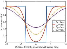
    Fig. 1. (Color online) Variation of Al component concentration with diffusion distance.
    (Color online) Variation of quantum well gain spectrum peaks with Al atom diffusion distances.
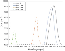
    Fig. 2. (Color online) Variation of quantum well gain spectrum peaks with Al atom diffusion distances.
    (Color online) The relationship between the interdiffusion coefficient of group III atoms and temperature.
    Fig. 3. (Color online) The relationship between the interdiffusion coefficient of group III atoms and temperature.
    (Color online) Schematic diagram of GaInP/AlGaInP QW semiconductor laser
    Fig. 4. (Color online) Schematic diagram of GaInP/AlGaInP QW semiconductor laser
    (Color online) PL spectrum of GaInP/AlGaInP quantum well laser. (a) The mapping results of PL testing. (b) PL spectrum of epitaxial layer.
    Fig. 5. (Color online) PL spectrum of GaInP/AlGaInP quantum well laser. (a) The mapping results of PL testing. (b) PL spectrum of epitaxial layer.
    (Color online) ECV test results of GaInP/AlGaInP quantum well epitaxial layer.
    Fig. 6. (Color online) ECV test results of GaInP/AlGaInP quantum well epitaxial layer.
    The process of lift-off technique.
    Fig. 7. The process of lift-off technique.
    (Color online) Sample surface after annealing at 580 °C/10 min.
    Fig. 8. (Color online) Sample surface after annealing at 580 °C/10 min.
    The PL spectrum under the annealing condition of 580 °C/10 min.
    Fig. 9. The PL spectrum under the annealing condition of 580 °C/10 min.
    (Color online) Schematic diagram after growing Si–Si3N4 composited dielectric layers.
    Fig. 10. (Color online) Schematic diagram after growing Si–Si3N4 composited dielectric layers.
    (Color online) The PL spectra at different annealing temperatures.
    Fig. 11. (Color online) The PL spectra at different annealing temperatures.
    (Color online) ECV test result of the sample annealed at 580 °C/10 min.
    Fig. 12. (Color online) ECV test result of the sample annealed at 580 °C/10 min.
    (Color online) The PL spectra of the samples after annealing different cycles.
    Fig. 13. (Color online) The PL spectra of the samples after annealing different cycles.
    SubstrateDielectric layerStress (MPa)
    GaAs100 nm Si3N4–1204.315
    GaAs100 nm Si–570.124
    Si100 nm Si3N4–755.056
    Table 1. Stress between dielectric layers.
    Tianjiang He, Suping Liu, Wei Li, Cong Xiong, Nan Lin, Li Zhong, Xiaoyu Ma. Research on quantum well intermixing of 680 nm AlGaInP/GaInP semiconductor lasers induced by composited Si–Si3N4 dielectric layer[J]. Journal of Semiconductors, 2022, 43(8): 082301
    Download Citation