
Tianjiang He, Suping Liu, Wei Li, Cong Xiong, Nan Lin, Li Zhong, Xiaoyu Ma. Research on quantum well intermixing of 680 nm AlGaInP/GaInP semiconductor lasers induced by composited Si–Si3N4 dielectric layer[J]. Journal of Semiconductors, 2022, 43(8): 082301
- Journal of Semiconductors
- Vol. 43, Issue 8, 082301 (2022)
Abstract
1. Introduction
Lasers, optical fibers and semiconductor photonic devices are generally regarded as the three major inventions in the field of optics in the twentieth century. Among them, semiconductor lasers play an important role in the whole laser field because of their small volume, light weight and easy integration[
Moreover, the device will fail in the range of tens of nanoseconds. An effective method to prevent this problem is to make a nonabsorbent window (NAW) at the laser cavity surface. As a post-treatment process, impurity induced quantum well hybrid technology has attracted extensive attention because of its advantages, such as easy process, low equipment requirements and low manufacturing cost. This research has been developed since it was found that the diffusion of Si impurities can promote the mutual diffusion of quantum barrier and quantum well components in the 1980s[
2. Establishing a quantum well intermixing model
2.1. Component calculation
For 680 nm single quantum well GaInP/Al0.53GaInP red semiconductor laser, Al, Ga and In atoms occupy group III lattice, while P atoms occupy group V lattice. Generally speaking, in III–V compound semiconductors, the two defects with the largest diffusion rate are group III vacancies VIIIand group III interstitial atoms IIII. The mutual diffusion of Al and Ga atoms is mainly considered in the process of component calculation and simulation because In atoms are large and have a slow diffusion rate. In the process of component interdiffusion caused by impurity induction, it is mainly carried out in the form of Frenkel defect pairs through ⅤIII and IIII[
The initial concentration of Al component is:
where Cw and Cb represent the component concentration of Al in the quantum well and quantum barrier, respectively. Taking the central position of the quantum well as the z-axis origin, the width of the quantum well is 2d.
Setting the diffusion length to Ld and after the completion of quantum well mixing, the expression of Al component concentration in quantum well and quantum barrier is as follows[
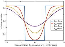
The width of the quantum well of the semiconductor laser epitaxial wafer used in this experiment is 7 nm, and the Al diffusion distance Ld is set to 0, 1, 2 and 3 nm. The Al component concentration can be calculated according to the diffusion distance after mixing, as shown in
![]()
Figure 1.(Color online) Variation of Al component concentration with diffusion distance.
From this figure it can be seen that when there is no diffusion, the content of Al in the well and barrier is 0 and 0.53, respectively. Meanwhile, the distribution of Al atoms in the well barrier shows an obvious step shape. When the diffusion length is short as Ld = 1 nm for example, Al occupies a relativeley large portion in the well region so the quantum well region and quantum barrier region can maintain good heterojunction morphology. However, with the increase of diffusion length, when Ld = 2 nm, the Al component concentration in the well region gradually increases, and the Al component concentration at the interface between the well region and the barrier region gradually tends to be consistent. When the diffusion length Ld reaches 3 nm, the Al composition in the well and barrier tends to be the same, the obvious interface between the well region and the barrier region has not been observed, and the heterojunction state is difficult to maintain. This figure also shows that the quantum well mixing degree between the well region and the barrier region has been sufficient.
2.2. Blue shift simulation
![]()
Figure 2.(Color online) Variation of quantum well gain spectrum peaks with Al atom diffusion distances.
It can be seen that when the diffusion distance is small—that is, the Al component changes little—, the gain spectrum peak basically has no blue shift and the value of gain has a small variation. However, when the diffusion distance gradually increases, the gain spectrum peak blue shift also increases, while the gain value decreases. A 40 nm of blue shift is observed when the diffusion distance is 2 nm and the gain value is 88.5% of the original value.
2.3. Effect of temperature on component interdiffusion
In group III–V semiconductors, the point defect concentration is usually much less than the group III atom concentration (about 2 × 1022 cm−3); that is, the mutual diffusion coefficient is mainly determined by the point defect concentration. The mutual diffusion coefficient is expressed as[
where DIII is the mutual diffusion coefficient of group III atoms, f1 and f2 are constants containing information about crystal structure and group III lattice concentration.
Assuming that there are N lattice points in group III lattice and the vacancy occupation number isn, then the possible arrangement number is
By using the Stirling formula, the Boltzmann entropy S can be written as:
and the free energy of the whole system can be expressed as:
where Ev is the energy required to form a vacancy, F0 is the partial free energy independent of the number of vacancies n, T is the temperature. In this system, the equilibrium is determined by minimizing the free energy and by taking the derivative of F to n we get
In this formula, the number of lattice points N is greater than vacancies n in the crystal. This can be simplified as:
Then, the normalized thermal equilibrium concentrations of group III vacancy and group III interstitial atoms are:
By introducing these two formulas, the expression of the mutual diffusion coefficient of group III atoms with temperature can be obtained:
From the
![]()
Figure 3.(Color online) The relationship between the interdiffusion coefficient of group III atoms and temperature.
3. Experimental process and analysis
3.1. Epitaxial structure
The 680 nm quantum well semiconductor laser used in this experiment was prepared on n-GaAs substrate by aix-200/4 system low-voltage MOCVD equipment. As shown in
![]()
Figure 4.(Color online) Schematic diagram of GaInP/AlGaInP QW semiconductor laser
Before manufacturing the experiment, it is essential to test the PL spectrum and Electrochemical Cyclic Voltammetry (ECV) of the epitaxial wafer, which shows the key information of light intensity, peak wavelength and carrier concentration, and carrier distribution. The test results are shown in
![]()
Figure 5.(Color online) PL spectrum of GaInP/AlGaInP quantum well laser. (a) The mapping results of PL testing. (b) PL spectrum of epitaxial layer.
![]()
Figure 6.(Color online) ECV test results of GaInP/AlGaInP quantum well epitaxial layer.
3.2. Effect of a single dielectric layer on quantum well intermixing
The lift-off technique process is adopted, as shown in
![]()
Figure 7.The process of lift-off technique.
The specific operation process is as follows. First, photolithography is carried out on the epitaxial wafer to form a gain luminescence region and nonabsorbent window region. Then, we sputter a layer of Si with sputtering equipment under the conditions of sputtering pressure of 1.3 Pa, sputtering power of 100 W, argon flow rate of 50 sccm and sputtering time of 30 min. By using the ellipsometry, the thickness and refractive index of Si dielectric layer were 100.85 nm and 3.4607, respectively. A whole epitaxial wafer was cut into 6 × 6 mm2 pieces followed by using rtp-500 rapid annealing furnace to handle these pieces. The annealing temperature was set to 540, 560 and 580 °C, while the annealing temperature remained unchanged for 10 min. After annealing, we remove the Si dielectric layer with KOH solution and observe the sample surface under the condition of annealing at 580 °C/10 min with a metallographic microscope, as shown in
![]()
Figure 8.(Color online) Sample surface after annealing at 580 °C/10 min.
From this figure it can be seen that the surface quality of the sample remained fine after annealing, while the PL spectra peak of Si covered region and non Si covered region were both 668.9 nm at these three temperatures. Taking the error of measurement into consideration, it can be considered that there is no blue shift.
![]()
Figure 9.The PL spectrum under the annealing condition of 580 °C/10 min.
It can be concluded that under this temperature range, quantum well intermixing could not happen if the condition is only simply thermal annealing[
3.3. Effect of composited dielectric layers on quantum well intermixing
![]()
Figure 10.(Color online) Schematic diagram after growing Si–Si3N4 composited dielectric layers.
Similarly, a wafer is cut into 6 × 6 mm2 small standard pieces, which were consequently annealed under the condition of 540–600 °C/10 min with the temperature gradient of 20 °C. We found that there was basically no blue shift in the Si3N4 covered region, while the PL spectrum of Si–Si3N4 covered region is shown in
![]()
Figure 11.(Color online) The PL spectra at different annealing temperatures.
It can be observed from this figure that with the gradual increase of annealing temperature, the wave peak of the spectrum gradually blue shifted. At 540 °C, the blue shift was 24 nm, while at 600 °C the blue shift reached 54.8 nm and the luminous intensity of all samples maintained more than 75% of the origin sample. This indicates that nonabsorbent window regions and gain luminescence regions were well realized.
An ECV test was carried out on the sample that was annealed at 580 °C/10 min, the result is shown in
![]()
Figure 12.(Color online) ECV test result of the sample annealed at 580 °C/10 min.
Compared with the ECV test result of the original sample, near 1.3 μm, the p-type doping concentration decreased while the n-type doping concentration increased. This indicates that Si impurities diffused into the sample and became n-type donors[
3.4. Effect of cyclic annealing
To avoid damage caused to the quantum well epitaxial wafer caused by long annealing time or high annealing temperature, we conducted three periods of annealing and the temperature of each period was 580 °C and the annealing time was 10 min. After one annealing period was completed and the temperature was cooled to room temperature, we repeated the same experiment three times. We then tested the PL spectrum for each time, as shown in
![]()
Figure 13.(Color online) The PL spectra of the samples after annealing different cycles.
It can be found from this figure that the luminescence intensity did not decrease significantly with the increase of cyclic annealing times, and the blue shifts were 42.9, 45.7 and 48 nm respectively from one to three annealing times. This demonstrates that under the condition of 580 °C/10 min cyclic annealing, even if it can promote the increase of blue shift, the increase was limited.
3.5. Stress between dielectric layers
A thin film stress tester was used to test the stress between dielectric layers, as shown in
The stress of 100 nm Si3N4 on GaAs substrate is –1204.315 MPa and the stress on Si substrate is –755.056 MPa, which is also relatively large. The surface compressive stress of GaAs will contribute to the generation of more Ga vacancy defects[
4. Conclusion
In this paper, we propose the use of Si–Si3N4 composited dielectric layers to induce quantum well intermixing of 680 nm red semiconductor lasers. Under the condition of low annealing temperature of 540–600 °C and annealing time of 10 min, the blue shift difference between nonabsorbent window region and gain luminescence region greater than 30 nm is well realized and the luminous intensities are also maintained at more than 75% of the original sample. Moreover, in this temperature range, only simple thermal annealing or growth of single Si dielectric layer will not cause quantum well intermixing, while the large stress exerted by Si3N4 will promote the diffusion of Si in GaAs during thermal annealing and induce quantum well intermixing. This method will not only ensure the good lattice quality of the epitaxial wafer surface but will also reduce the process difficulty, which is conducive to the later device fabrication and provides an effective scheme to improve the COD threshold of 680 nm band semiconductor lasers.
Acknowledgements
This work was supported by the National Natural Science Foundation of China (NNSFC) (Grant No.62174154).
References
[4] Y Sin, N Ives, S LaLumondiere et al. Catastrophic optical bulk damage (COBD) in high power multi-mode InGaAs-AlGaAs strained quantum well lasers. High-Power Diode Laser Technology and Applications IX, 791803(2011).
[7] T J He, H Q Jing, L N Zhu et al. Research on quantum well intermixing of 915 nm InGaAsP/GaAsP primary epitaxial wafers. Acta Opt Sinica, 42, 0114003(2022).
[11] H T Peng. Improving the COD level of high-power semiconductor lasers using quantum well intermixing(2007).
[13] J T Zhou, H L Zhu, Y B Cheng et al. Low energy helium ion implantation induced quantum-well intermixing. J Semicond, 28, 47(2007).
[14] X H Ge, R Y Zhang, C Y Guo et al. Stduy of multiple factors ion-implantation-induced quantum wells intermixing. Laser Optoelectron Prog, 57, 7(2020).
[15] X H Fang, X M Bao. Study on mechanism of Si diffusion in GaAs. J Semicond, 922(1996).
[18] L Zhou. Research on anti catastrophic optical damage of high power semiconductor laser diodes(2014).
[23] C C Liu, N Lin, X Y Ma et al. High performance InGaAs/AlGaAs quantum well semiconductor laser diode with non-absorption window. Chin J Lumin, 43, 9(2022).

Set citation alerts for the article
Please enter your email address
© Copyright 2018-2021 | Chinese Laser Press. All Rights Reserved 沪ICP备15018463号-20