
Jiahe Chai, Mingli Dong, Peng Sun, Bixi Yan. Model and compensation method of image point drift caused by self-heating of industrial camera[J]. Infrared and Laser Engineering, 2021, 50(6): 20200494
- Infrared and Laser Engineering
- Vol. 50, Issue 6, 20200494 (2021)
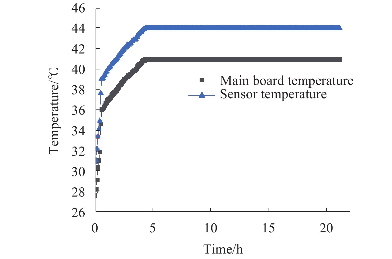
Fig. 1. Temperature change of the imaging device and the main board after turning on
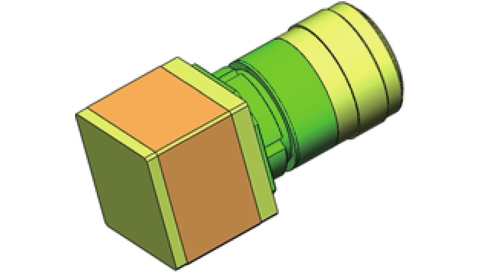
Fig. 2. 3D model of AVT GT5120 camera
Fig. 3. Camera finite element model
Fig. 4. Camera transient thermal stress analysis results
Fig. 5. Axial offset of the camera causes the imaging optical path to change
Fig. 6. Image point drift caused by axial optical path changes
Fig. 7. Schematic diagram of image point shift caused by radial expansion
Fig. 8. Temperature changes of the experimental device and its components
Fig. 9. In the self-heating state, the coordinate value of each quadrant point after compensation is compared with the experimental measurement value
Fig. 10. Camera thermal control system
|
Table 1. Material properties of camera components
|
Table 2. Deformation of the lens and CMOS under different temperature variation
| ||||||||||||||||||||||||||||||||||||||||||
Table 3. Pixel drift compensation model error
| ||||||||||||||||||||||||||||||||||||||||||
Table 4. Comparison of thermal control device method and image point drift compensation method


Set citation alerts for the article
Please enter your email address

© Copyright 2018-2021 | Chinese Laser Press. All Rights Reserved 沪ICP备15018463号-20