
Lufeng Liao, Sikun Li, Xiangzhao Wang, Libin Zhang, Shuang Zhang, Pengzheng Gao, Yayi Wei, Weijie Shi. Critical Pattern Selection Based on Diffraction Spectrum Analysis for Full-Chip Source Mask Optimization[J]. Acta Optica Sinica, 2020, 40(21): 2122001
- Acta Optica Sinica
- Vol. 40, Issue 21, 2122001 (2020)
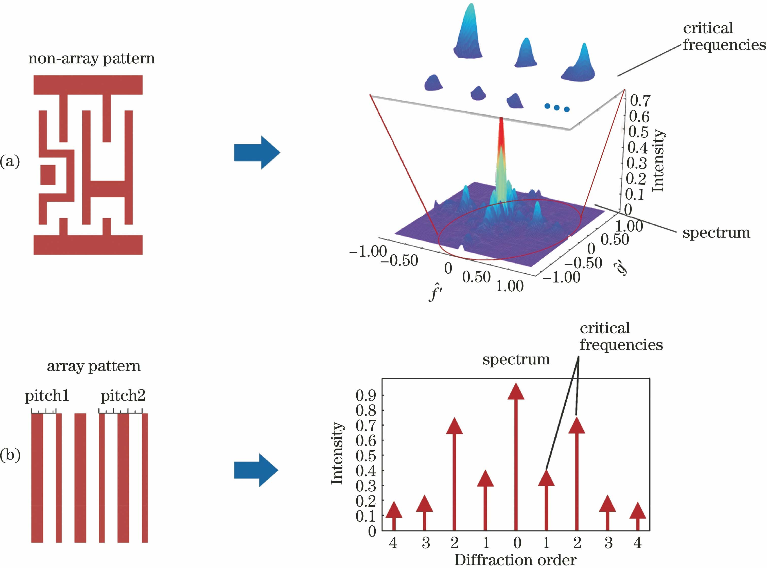
Fig. 1. Extraction principle of critical frequency of pattern. (a) Non-array pattern; (b) array pattern
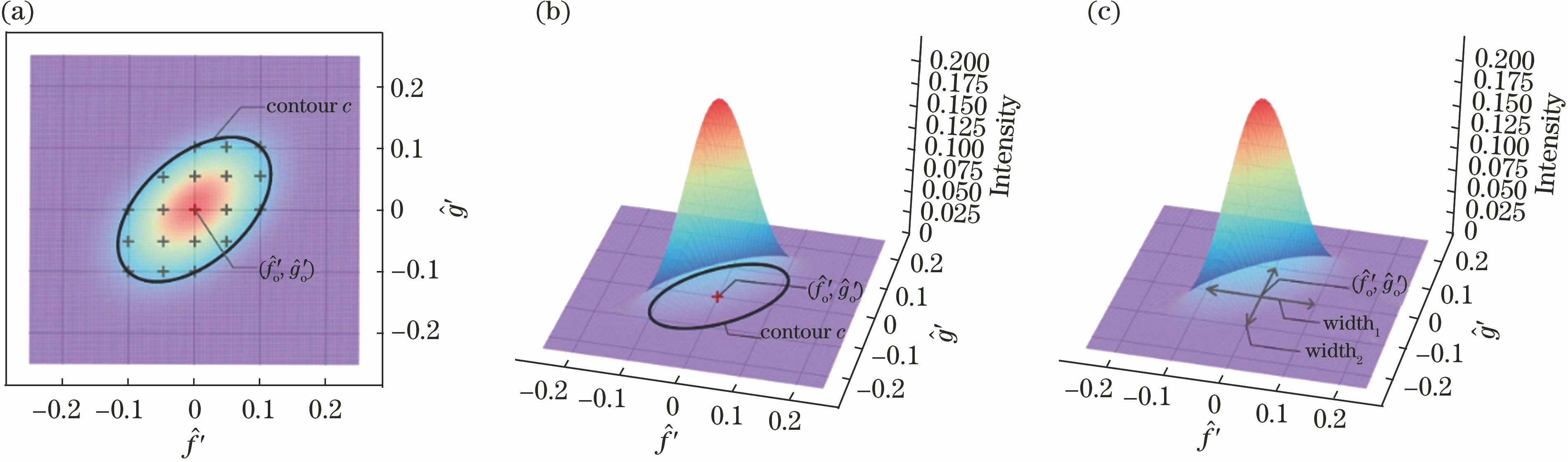
Fig. 2. Schematic diagram of critical frequency. (a) Critical frequency's contour on the frequency plane; (b) description method for critical frequency of our method; (c) description method for critical frequency of ASML Tachyon method
Fig. 3. Schematic diagram of the coverage relationship between critical frequencies
Fig. 4. Flow chart of the critical frequency grouping method
Fig. 5. Flow chart of the critical pattern selection method
Fig. 6. Critical pattern selection result of our method (pattern set A, repeating case)
Fig. 7. Critical pattern selection result of ASML Tachyon method (pattern set A, repeating case)
Fig. 8. Optimized sources obtained after SMO is performed on two methods' critical pattern selection results. (a) Our method; (b) ASML Tachyon method (pattern set A, repeating case)
Fig. 9. Process windows obtained after MO is performed on all patterns by using the two sources. (a) Common process windows; (b) EL versus DOF curves (pattern set A, repeating case)
Fig. 10. Critical pattern selection result of our method (pattern set A, unrepeating case)
Fig. 11. Critical pattern selection result of ASML Tachyon method (pattern set A, unrepeating case)
Fig. 12. Optimized sources obtained after SMO is performed on critical pattern selection results. (a) Our method; (b) ASML Tachyon method (pattern set A, unrepeating case)
Fig. 13. Process windows obtained after MO is performed on all patterns by using the two sources. (a) Common process windows; (b) EL versus DOF curves (pattern set A, unrepeating case)
Fig. 14. Critical patterns obtained by two methods (pattern set B)
Fig. 15. Simulation results (pattern set B)
|
Table 1. Simulation setting
|
Table 2. DOF, maximum MEEF and worst ILS obtained by the two methods (pattern set A, repeating case)
|
Table 3. DOF, maximum MEEF and worst ILS obtained by the two methods (pattern set A, unrepeating case)

Set citation alerts for the article
Please enter your email address
© Copyright 2018-2021 | Chinese Laser Press. All Rights Reserved 沪ICP备15018463号-20