• Journal of Semiconductors
  • Vol. 41, Issue 4, 042602 (2020)
Guozhen Shen1、2, Haoran Chen1、2, and Zheng Lou1
Author Affiliations
  • 1State Key Laboratory for Superlattices and Microstructures, Institute of Semiconductors, Chinese Academy of Sciences, Beijing 100083, China
  • 2Center of Materials Science and Optoelectronic Engineering, University of Chinese Academy of Sciences, Beijing 100049, China
  • show less
    DOI: 10.1088/1674-4926/41/4/042602 Cite this Article
    Guozhen Shen, Haoran Chen, Zheng Lou. Growth of aligned SnS nanowire arrays for near infrared photodetectors[J]. Journal of Semiconductors, 2020, 41(4): 042602 Copy Citation Text show less
    (Color online) (a, b) SEM images, (c) XRD pattern, (d) TEM image, (e) SAED pattern and (f) HRTEM image of the synthesized SnS nanowires.
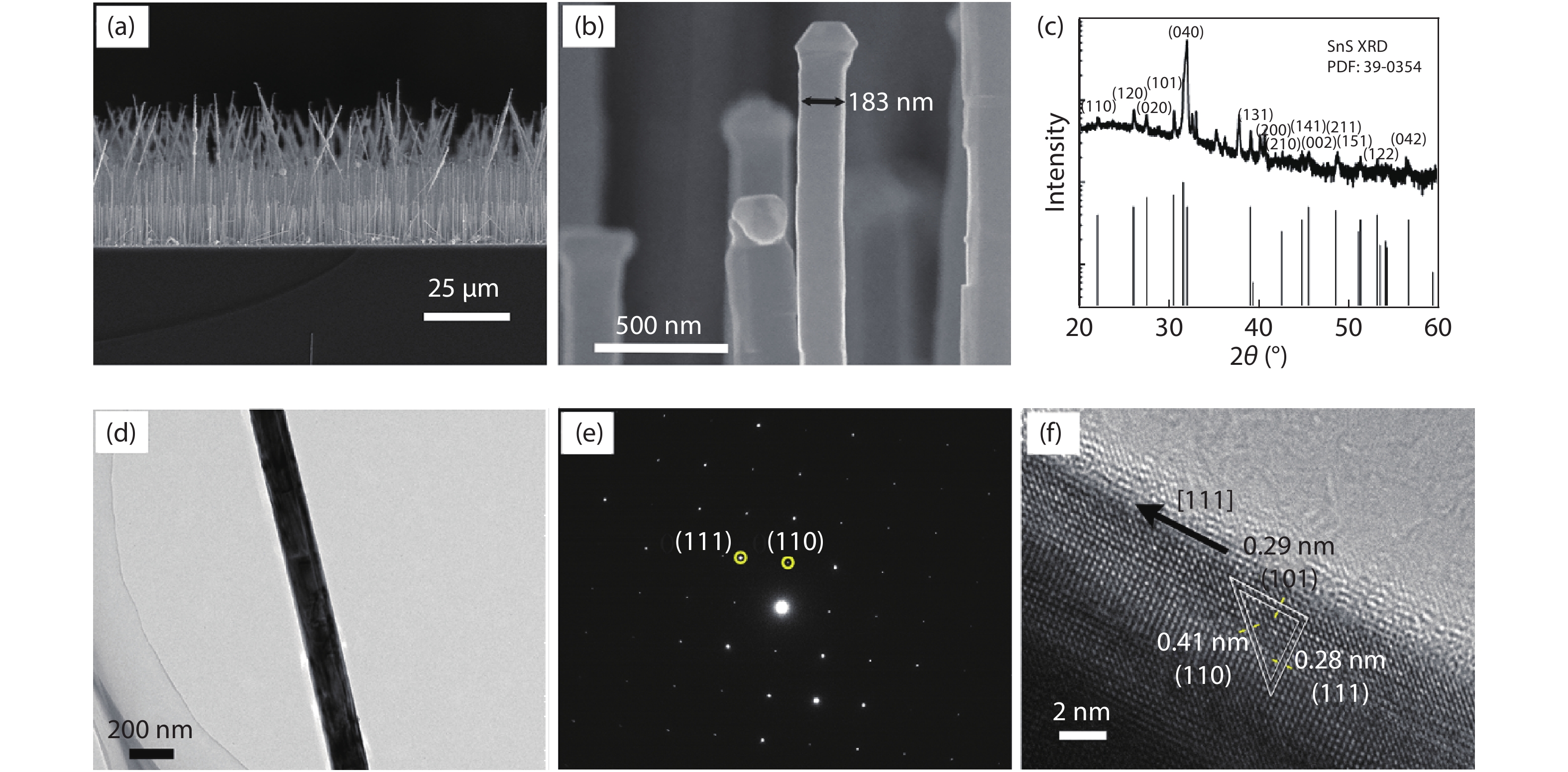
    Fig. 1. (Color online) (a, b) SEM images, (c) XRD pattern, (d) TEM image, (e) SAED pattern and (f) HRTEM image of the synthesized SnS nanowires.
    (Color online) Characterizations of the single SnS nanowire based photodetector. (a) SEM image of a single nanowire device. (b) I–V curves of the device to NIR lights of 808, 915, 1064 and 1342 nm, respectively. (c) I–V curves of the device to 1064 nm lights with different light intensities. (d) Light intensity dependent photocurrent at a fixed bias voltage of 3 V. (e) The reproducible and stable switching behavior of the device to 1064 nm light. (f) Transient response and decay time of the device.
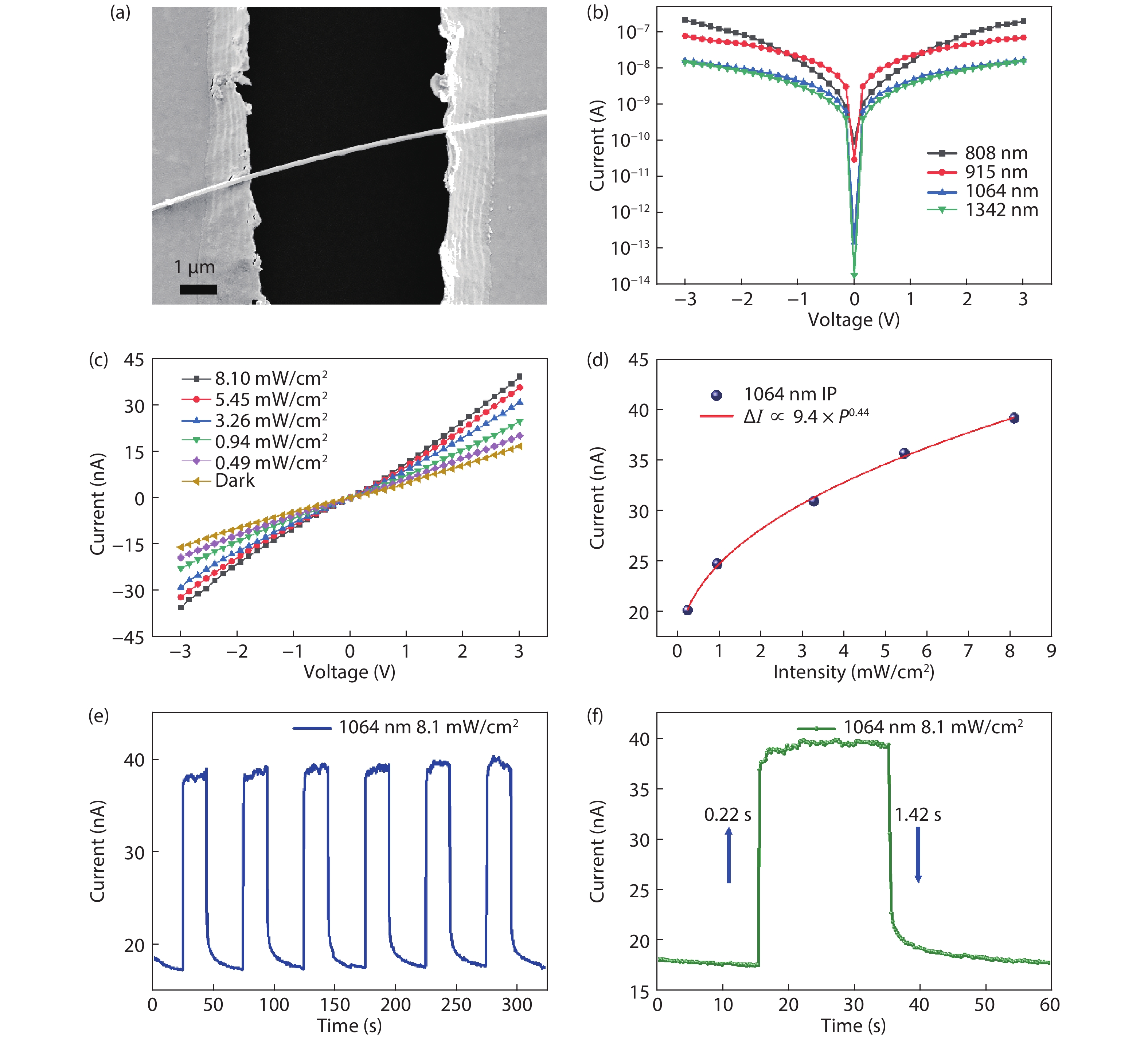
    Fig. 2. (Color online) Characterizations of the single SnS nanowire based photodetector. (a) SEM image of a single nanowire device. (b) I–V curves of the device to NIR lights of 808, 915, 1064 and 1342 nm, respectively. (c) I–V curves of the device to 1064 nm lights with different light intensities. (d) Light intensity dependent photocurrent at a fixed bias voltage of 3 V. (e) The reproducible and stable switching behavior of the device to 1064 nm light. (f) Transient response and decay time of the device.
    (Color online) (a) Schematic of the fabrication process of the aligned SnS nanowire arrays based photodetectors. (b) SEM images of the aligned SnS nanowires deposited with PMMA and Ag nanowires.
    Fig. 3. (Color online) (a) Schematic of the fabrication process of the aligned SnS nanowire arrays based photodetectors. (b) SEM images of the aligned SnS nanowires deposited with PMMA and Ag nanowires.
    (Color online) Characterizations of the aligned SnS nanowire array based photodetectors. (a) I–V curves of the nanowire array device to NIR lights with different wavelengths. (b) I–V curves of the device to 1064 nm lights with different light intensities. (c) Reproducible and stable switching behavior of the device to 1064 nm light. (d) Transient response and decay time of the device.
    Fig. 4. (Color online) Characterizations of the aligned SnS nanowire array based photodetectors. (a) I–V curves of the nanowire array device to NIR lights with different wavelengths. (b) I–V curves of the device to 1064 nm lights with different light intensities. (c) Reproducible and stable switching behavior of the device to 1064 nm light. (d) Transient response and decay time of the device.
    Guozhen Shen, Haoran Chen, Zheng Lou. Growth of aligned SnS nanowire arrays for near infrared photodetectors[J]. Journal of Semiconductors, 2020, 41(4): 042602
    Download Citation