
Guozhen Shen, Haoran Chen, Zheng Lou. Growth of aligned SnS nanowire arrays for near infrared photodetectors[J]. Journal of Semiconductors, 2020, 41(4): 042602
- Journal of Semiconductors
- Vol. 41, Issue 4, 042602 (2020)
Abstract
1. Introduction
Orthorhombic tin sulfide (SnS) is an important member of anisotropic layered IV–VI group semiconductors, where Sn atoms are coordinated to three S atoms to form the puckered Sn–S layers coupled by weak van der Waals forces[
Nanowire (NW) arrays have the characteristics of large effective irradiation area, the multiple scattering of incident light, and the increased path length of incident light. Using NW arrays to trap light provides an effective way to improve the absorption capacity of photoelectric devices[
In this work, we report the preparation of aligned SnS NW arrays using chemical vapor deposition method. As-grown individual SnS NW exhibited excellent response to near infrared lights with good responsivity of 267.9 A/W, high external quantum efficiency of 3.12 × 10⁴ % and fast response time. Photodetectors constructed from the aligned SnS NW arrays were demonstrated to be capable to detect NIR lights (808–1450 nm) with the photocurrent enhanced about 5 times compared with single NW.
2. Experimental
Aligned SnS NW arrays were synthesized via a simple chemical vapor deposition method. In a typical process, high purity SnS powders (99.5%, Alfa) were put into a ceramic boat, which was placed in the center of a quartz tube of a tube furnace. The silicon substrate covered with a thin layer of Au film (10 nm) was placed at the downstream about 1–2 cm away from the boat. The furnace was first purged with high purity Ar gas for 30 min and then heated to 750 °C and kept at that temperature for 30 min. After cooling down to room temperature, a layer of black powders was found deposited on the whole substrate.
The prepared samples were characterized using scanning electron microscope (SEM, FEI NanoSEM650), transmission electron microscope (TEM, JEM-2100F) equipped with an X-ray energy dispersive spectrometer (EDS) and X-ray diffractometry (XRD, Rigaku D/Max-2550).
To investigate the optoelectronic properties, the as-grown SnS nanowires were dispersed into isopropanol (IPA) and dropped onto SiO2/Si substrates. Standard photolithography was then performed to pattern the electrode. 100 nm Au was then deposited on the terminals of a single SnS NW as the source and drain electrodes. The corresponding measurements were carried out with a probe station connected with a Keysight B1500A semiconductor characterization system. Near infrared lasers with different wavelengths and tunable light intensities were adopted as the illumination source. All measurements were carried out in air at room temperature.
3. Results and discussions
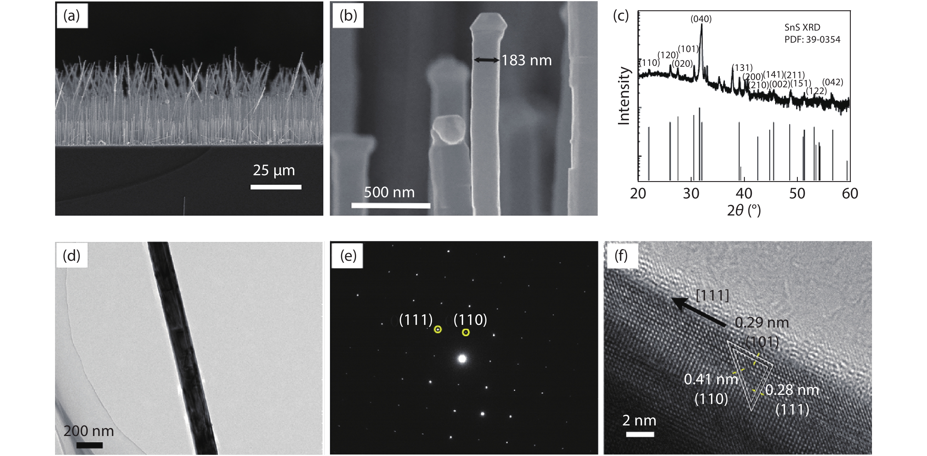
Fig. 1(a) showed the cross-section view SEM image of the sample deposited on Si substrate. High density nanowires were found aligned on the substrate, forming into aligned NW arrays. Typical NWs have the diameters ranging from 100 to 300 nm. High-resolution SEM image of a single NW was shown in Fig. 1(b), where the NW has a diameter of 183 nm with smooth surface. Nanoparticle was found on top of the NW, indicating typical vapor–liquid–solid (VLS) growth mechanism[
![]()
Figure 1.(Color online) (a, b) SEM images, (c) XRD pattern, (d) TEM image, (e) SAED pattern and (f) HRTEM image of the synthesized SnS nanowires.
To study the photoresponse properties of the synthesized SnS sample, single NW device was first fabricated via a conventional photolithography and lift-off process, according to our previous reports[
![]()
Figure 2.(Color online) Characterizations of the single SnS nanowire based photodetector. (a) SEM image of a single nanowire device. (b)
Response time and decay time are the key parameters to measure the response speed of a photodetector. Generally, the response time is defined as the time taken for the current of the device to increase from 10% to 90% of the peak value, while the decay time is defined to be the opposite[
The responsivity (Rλ) and the external quantum efficiency (EQE) are important parameters to evaluate a photodetector. They can be defined as[
In these equations, P is the power intensity of the incident light, S is the effective illumination area, Iphoto and Idark are the photo current and the dark current, h is the Planck’s constant, c is the velocity of incident light, e is the elementary electronic charge, and λ is the wavelength of incident light. According to these equations, under 1064 nm light illumination with the light intensity of 8.1 mW/cm2, the responsivity and EQE are calculated to be 267.9 A/W and 3.12 × 10⁴ %, respectively. The specific detectivity (D*) is another important parameter for a photodetector, which can be defined as follows[
where Rλ is responsivity, and Δf is the band width. From the data in Fig. 2, the D* was calculated to be around 3.63 × 10¹¹ J.
As the synthesized SnS NWs exhibited excellent photoresponse to NIR illumination, we then fabricated photodetectors based on the aligned SnS NW arrays. Fig. 3(a) demonstrated the schematic illustration of the typical fabrication process. Briefly, silicon substrate was coated with a layer of Au film to grow the aligned SnS NW arrays. After the growth, a layer of polymethyl methacrylate (PMMA) was spin-coated on the NW arrays. Silver NWs were then coated on the PMMA layer, acting as one electrode of the device. In this structure, PMMA was used to avoid the direct contact of Ag NWs with Si, another electrode of the device. The corresponding SEM images of the devices were shown in Figs. 3(b) and 3(c), clearly illustrating the coating of Ag NWs and PMMA on the SnS NW arrays (marked with arrows).
![]()
Figure 3.(Color online) (a) Schematic of the fabrication process of the aligned SnS nanowire arrays based photodetectors. (b) SEM images of the aligned SnS nanowires deposited with PMMA and Ag nanowires.
The photoresponse performance of the aligned NW arrays based photodetectors were then measured at room temperature. Fig. 4(a) gave the I–V curves of the device to NIR lights with different wavelengths as well as in dark condition. Similar to single SnS NW, the NW arrays based photodetectors exhibited obvious response to NIR lights with light wavelengths ranging from 808 to 1450 nm. As the direct bandgap of SnS is 1.1 eV, we then studied the photoresponse of the SnS NW arrays based photodetector to the NIR light with the wavelength of 1064 nm in detail. Photoresponse of the device to 1064 nm light with different light intensities was shown in Fig. 4(b). The photocurrents were found increased gradually with increased light intensities and their relationship was plotted as ΔI ~ 2.38 × P0.89 (Fig. 4(b) inset). For photodetectors, stability is one of the key factors for their practical applications. The repeatability and response speed of the NW arrays based devices were thus studied. Fig. 4(c) depicted the dynamic current-time curves of the device to 1064 nm light at a fixed light intensity of (17.94 mW/cm2). It was found that, under same conditions, both the photocurrent and the Ion/Ioff ratio of the aligned SnS NW arrays based device were largely improved compared with those of single SnS NW based device, indicating the improvement of light absorbing ability of the NW arrays[
![]()
Figure 4.(Color online) Characterizations of the aligned SnS nanowire array based photodetectors. (a)
4. Conclusion
In conclusion, we successfully synthesized aligned SnS NW arrays via a simple chemical vapor deposition method. As-growth NWs exhibited excellent response to near infrared lights in terms of good responsivity, high external quantum efficiency and fast response time. Photodetectors were built on the aligned SnS NW arrays. Due to the light trapping ability of the aligned NW arrays, both the photocurrent and the Ion/Ioff ratio of the aligned SnS NW arrays based device were largely improved compared with their single SnS NW counterpart. By using direct transfer method, flexible photodetectors are expected to be fabricated for next generation flexible electronic applications and related work is still in progress.
Acknowledgements
This work was financial supported by National Natural Science Foundation of China (61625404, 61888102).
References
[1] V Steinmann, R Jaramillo, K Hartman et al. 3.88% efficient tin sulfide solar cells using congruent thermal evaporation. Adv Mater, 26, 7488(2014).
[2] L Zhao, G Tan, S Hao et al. Ultrahigh power factor and thermoelectric performance in hole-doped single-crystal SnSe. Science, 351, 141(2016).
[3] T Rath, L Gury, I Sanchez-Molina et al. Formation of porous SnS nanoplate networks from solution and their application in hybrid solar cells. Chem Commun, 51, 10198(2015).
[4] G M Kumar, X Fu, P Ilanchezhiyan et al. Highly sensitive flexible photodetectors based on self-assembled tin monosulfide nanoflakes with graphene electrodes. ACS Appl Mater Interface, 9, 32142(2017).
[5] Y Lin, X Wen, L Wang et al. Structure and optical properties of SnS nanowire arrays prepared with two-step method. Adv Mater Res, 476, 1519(2012).
[6] X Zhou, L Gan, Q Zhang et al. High performance near-infrared photodetectors based on ultrathin SnS nanobelts grown via physical vapor deposition. J Mater Chem C, 4, 2111(2016).
[7] D Zheng, H Fang, M Long et al. High-performance near-infrared photodetectors based on p-type SnX (X = S, Se) nanowires grown via chemical vapor deposition. ACS Nano, 12, 7239(2018).
[8] J Chao, Z Wang, X Xu et al. Tin sulfide nanoribbons as high performance photoelectrochemical cells, flexible photodetectors and visible-light-driven photocatalysts. RSC Adv, 3, 2746(2013).
[9] Z Zhang, J Yang, K Zhang et al. Anisotropic photoresponse of layered 2D SnS-based near infrared photodetectors. J Mater Chem C, 5, 11288(2017).
[10] Z Deng, D Cao, J He et al. Solution synthesis of ultrathin single-crystalline SnS nanoribbons for photodetectors via phase transition and surface processing. ACS Nano, 6, 6197(2012).
[11] L Ning, T Jiang, Z Shao et al. Light-trapping enhanced ZnO-MoS2 core-shell nanopillar arrays for broadband ultraviolet-visible-near infrared photodetection. J Mater Chem C, 6, 7077(2018).
[12] D Zhang, L Gu, Q Zhang et al. Increasing photoluminescence quantum yield by nanophotonic design of quantum-confined halide perovskite nanowire arrays. Nano Lett, 19, 2850(2019).
[13] L Gu, M M Tavakoli, D Zhang et al. 3D arrays of 1024-pixel image sensors based on lead halide perovskite nanowires. Adv Mater, 28, 9713(2016).
[14] Z Fan, R Kapadia, P Leu et al. Ordered arrays of dual-diameter nanopillars for maximized optical absorption. Nano Lett, 10, 3823(2010).
[15] Z Fan, H Razzavi, J Do et al. Three-dimensional nanopillar-array photovoltaics on low-cost and flexible substrate. Nat Mater, 8, 648(2009).
[16] X Duan, C M Lieber. General synthesis of compound semiconductor nanowires. Adv Mater, 12, 298(2000).
[17] Y Wu, g P Yang. Direct observation of vapor-liquid-solid nanowire growth. J Am Chem Soc, 123, 3165(2001).
[18] G Shen, J Xu, X Wang et al. Growth of directly transferrable In2O3 nanowire mats for transparent thin-film transistors applications. Adv Mater, 23, 771(2011).
[19] T Luo, B Liang, Z Liu et al. Single-GaSb-nanowire-based room temperature photodetectors with broad spectral response. Sci Bull, 60, 101(2015).
[20] T Duan, Z Lou, G Shen. Electrical transport and photoresponse properties of single-crystalline Cd3As2 nanowires. Sci China-Phys Mech Astron, 58, 027801(2015).
[21] L Li, Z Lou, G Shen. Flexible broadband image sensors with SnS quantum dots/Zn2SnO4 nanowires hybrid nanostructures. Adv Funct Mater, 18, 1705389(2018).
[22] S Chen, Z Lou, D Chen et al. Printble Zn2GeO4 microwires based flexible photodetectors with tunable photorespone. Adv Mater Technol, 3, 1800050(2018).
[23] Z Lou, L Li, G Shen. InGaO3(ZnO) superlattice nanowires for high performance ultraviolet photodetectors. Adv Electron Mater, 1, 1500054(2015).
[24] Z Lou, X L Yang, H R Chen et al. Flexible ultraviolet photodetectors based on ZnO–SnO2 heterojunction nanowire arrays. J Semicond, 39, 024002(2018).
[25] G Chen, B Liang, X Liu et al. High-performance hybrid phenyl-C61-butyric acid methyl ester/Cd3P2 nanowire ultraviolet-visible-near infrared photodetectors. ACS Nano, 8, 787(2014).
[26] Z Lou, L Li, G Shen. Ultraviolet/visible photodetectors with ultrafast, high photosensitivity based on 1D ZnS/CdS heterostructures. Nanoscale, 8, 5219(2016).
[27] R Chai, Z Lou, G Shen. Highly flexible self-powered photodetectors based on core-shell Sb/CdS nanowires. J Mater Chem C, 7, 4581(2019).
[28] Z Liu, T Luo, B Liang et al. High-detectivity InAs nanowire photodetectors with spectral response from ultraviolet to near-infrared. Nano Res, 6, 775(2013).
[29] X Gong, M Tong, Y Xia et al. High-detectivity polymer photodetectors with spectral response from 300 nm to 1450 nm. Science, 325, 1665(2009).
[30] J Miao, W Hu, N Guo et al. Single InAs nanowire room temperature near-infrared photodetectors. ACS Nano, 8, 3628(2014).
[31] B Ouyang, K Zhang, Y Yang et al. Photocurrent polarity controlled by light wavelength in self-powered ZnO nanowires/SnS photodetector system. iScience, 1, 16(2018).
[32] G Chen, B Liang, Z Liu et al. High performance rigid and flexible visible-light photodetectors based on aligned X(In,Ga)P nanowire arrays. J Mater Chem C, 2, 1270(2014).

Set citation alerts for the article
Please enter your email address
© Copyright 2018-2021 | Chinese Laser Press. All Rights Reserved 沪ICP备15018463号-20