
Xin Li, Wei Gao, Liangjun Lu, Jianping Chen, Linjie Zhou, "Ultra-low-loss multi-layer 8 × 8 microring optical switch," Photonics Res. 11, 712 (2023)
- Photonics Research
- Vol. 11, Issue 5, 712 (2023)
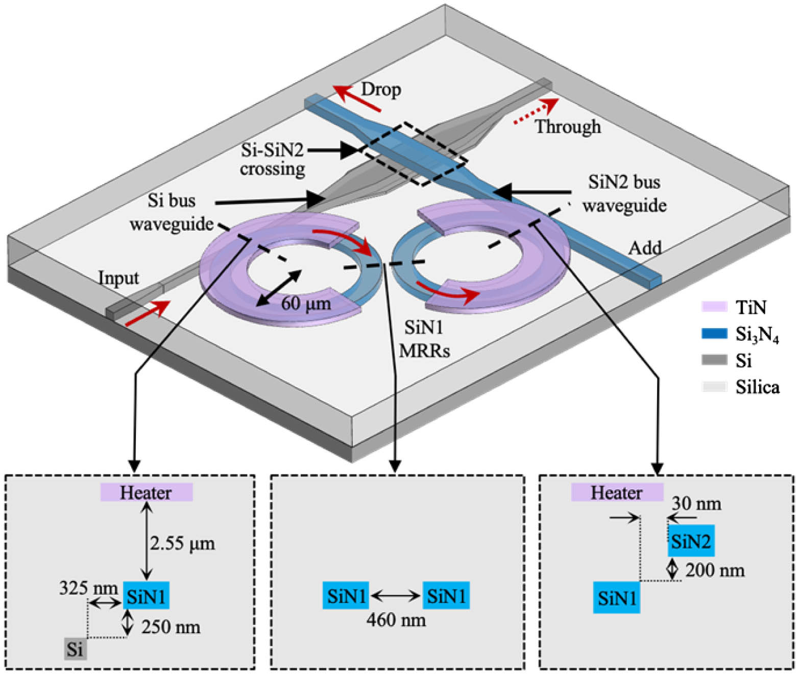
Fig. 1. Schematic of the 2 × 2
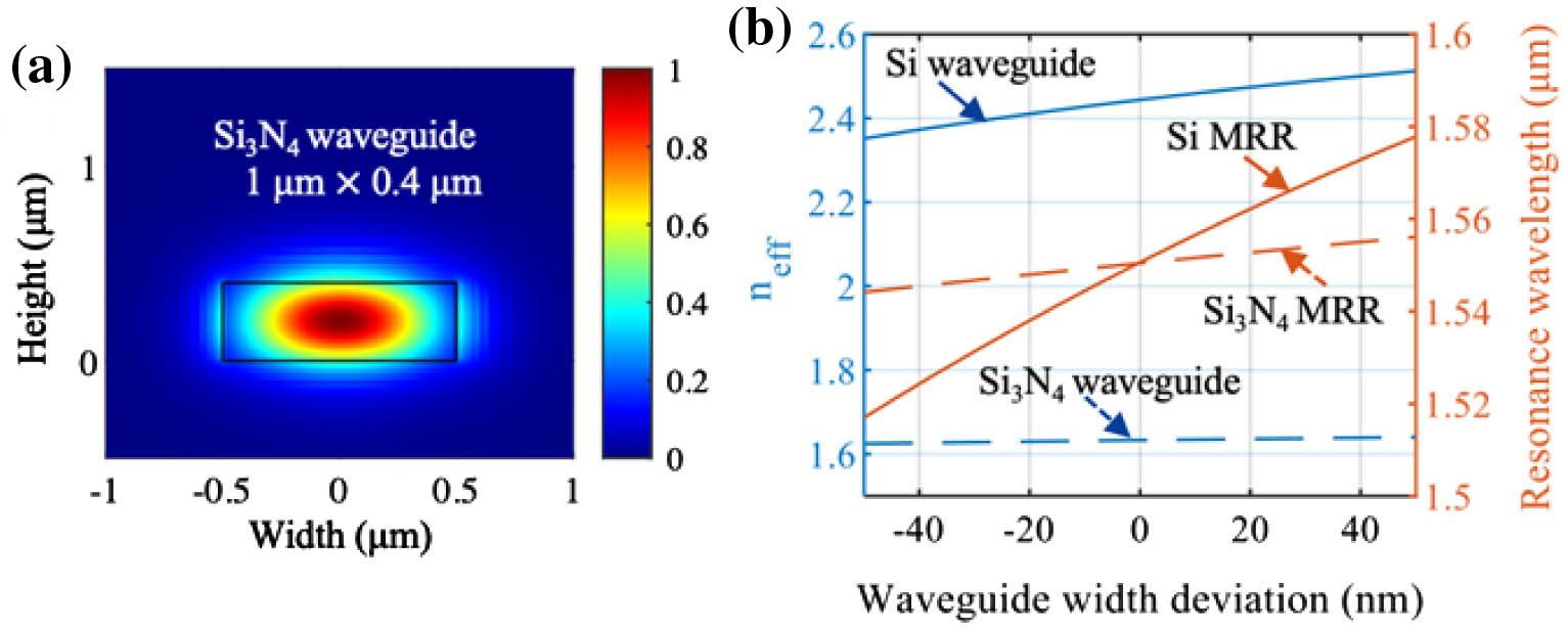
Fig. 2. (a) Electric-field intensity profile of the Si 3 N 4 1 μm × 0.4 μm Si 3 N 4 0.5 μm × 0.22 μm
Fig. 3. (a) General port arrangement of the 8 × 8 SE 54 I 5 I 5 * O 4 O 4 *
Fig. 4. (a) Microscope image of the fabricated 8 × 8 2 × 2 Si - Si 3 N 4
Fig. 5. (a) and (b) Through-transmission spectra of the 8 × 8 I 1
Fig. 6. (a), (b) Transmission spectra of the routing paths of (a) I i → O j I i * → O j * I i → O j I i * → O j * i j = 1 , 2 , … , 8
Fig. 7. Transmission spectra of the target path and the leakages from other input ports for (a) the routing path I 8 → O 4 I 1 → O 3 ER on ER off ER off ER on
Fig. 8. Fiber-to-fiber ILs of all target ports at the wavelength of 1563 nm; 63 solid circles represent paths of I i → O j i j = 1 , 2 , … , 8 I i * → O j *
Fig. 9. (a), (b) Heatmap of the on-chip ILs for path (a) I → Os I * → O * s
Fig. 10. (a) Schematic of a non-duplicate polarization-diversity 8 × 8
Fig. 11. (a) PDLs and DGDs for eight representative paths. (b), (c) Electrical signal responses for (b) path 1 → 1 * 6 → 6 *
Fig. 12. Experimental setup for 100 Gb/s DP-QPSK signal transmission over the polarization-diversity 8 × 8
Fig. 13. Constellation diagrams in the back-to-back (B 2 B 1 → 1 *
Fig. 14. Curve fitting results of eight representative diagonal SEs of the switch fabric. The solid blue and red lines represent the measured transmission spectra of I i → O i I i * → O i * i = 1 , 2 , … , 8
Fig. 15. (a), (c), (e) Heatmaps and (b), (d), (f) corresponding histograms of extracted (a), (b) on-state loss, (c), (d) off-state loss from the Si waveguide direction, and (e), (f) off-state loss from the SiN2 waveguide direction of all the SEs in the chip.
Fig. 16. (a), (b) Extra loss fitting for (a) the horizontal Si waveguide transmission and (b) the vertical SiN2 waveguide transmission.
Fig. 17. (a) Interlayer waveguide coupling coefficient, (b) on- and off-state IL and (c) ER off
|
Table 1. Characteristics Comparison of MRR-Based Photonic Switches


Set citation alerts for the article
Please enter your email address

© Copyright 2018-2021 | Chinese Laser Press. All Rights Reserved 沪ICP备15018463号-20