1State Key Laboratory of Advanced Optical Communication Systems and Networks, Shanghai Key Laboratory of Navigation and Location Services, Shanghai Institute for Advanced Communication and Data Science, Department of Electronic Engineering, Shanghai Jiao Tong University, Shanghai 200240, China
2SJTU-Pinghu Institute of Intelligent Optoelectronics, Pinghu 314200, China
Microring-based optical switches are promising for wavelength-selective switching with the merits of compact size and low power consumption. However, the large insertion loss, the high fabrication, and the temperature sensitivity hinder the scalability of silicon microring optical switch fabrics. In this paper, we utilize a three-dimensional (3D) microring-based optical switch element (SE) on a multi-layer -on-SOI platform to realize high-performance large-scale optical switch fabrics. The 3D microring-based SE consists of a waveguide overpass crossing in the bottom and the top layers, and dual-coupled microring resonators (MRRs) in the middle layer. The switch is calibration-free and has low insertion loss. With the 3D microring-based SEs, we implement an crossbar optical switch fabric. As the resonance wavelengths of all SEs are well aligned, only one SE needs to be turned on in each routing path, which greatly reduces the complexity of the switch control. The optical transmission spectra show a box-like shape, with a passband width of and an average on-state loss of . The chip has a record-low on-chip insertion loss of 0.52–2.66 dB. We also implement a non-duplicate polarization-diversity optical switch by using the bidirectional transmission characteristics of the crossbar architecture, which is highly favorable for practical applications. 100 Gb/s dual-polarization quadrature-phase-shift-keying (DP-QPSK) signal is transmitted through the switch without significant degradation. To the best of our knowledge, this is the first time that 3D MRRs have been used to build highly scalable polarization-diversity optical switch fabrics.
1. INTRODUCTION
Due to the rapid development of information technologies such as cloud computing, Internet of things (IoT), and artificial intelligence (AI), data traffic is increasing explosively. While wavelength division multiplexing (WDM)-based optical communications have greatly improved the data transmission bandwidth, the switching capacity of the switching nodes is still limited due to electronic bottlenecks [1]. Data switching in the optical domain can take advantage of the high-speed and broadband optical communication capability, which is highly demanded in future optical switching networks [2,3]. The large-scale optical switch fabric is one of the key components in optical switching networks. The silicon photonics platform shows the merits of high integration density, low power consumption, and compatibility with complementary metal–oxide semiconductor (CMOS) processes, which are well-suited for large-scale optical switch fabrics [4–6].
Silicon-based optical switches have made tremendous breakthroughs in recent years [7–24]. Most of the demonstrated silicon optical switch fabrics are based on Mach–Zehnder interferometers (MZIs) [8–13]. The MZI-based switches typically have a wide optical bandwidth but tend to be large and consume high power. Conversely, microring resonator (MRR)-based optical switches have a compact size, have low power consumption, and are better suited for WDM systems due to their wavelength selectivity. However, the port counts of the reported silicon-based integrated MRR switch fabrics are much smaller than those of the MZI-based switch fabrics [14–24].
There are some limitations to large-scale silicon MRR switches. First of all, the optical mode in a silicon single-mode waveguide (typical width of 500 nm) is very sensitive to the waveguide width due to the large modal overlap with the waveguide sidewalls. Waveguide width deviation due to fabrication imperfections results in the relatively random distribution of the MRRs’ resonances in the switch fabrics [25]. Therefore, wavelength calibration is indispensable for all MRRs in the switch fabrics. Although expanding the waveguide width can reduce the phase errors of silicon MRRs [26,27], the curved waveguides should be carefully designed to suppress higher modes for such multimode waveguides. Second, the large thermo-optic (TO) coefficient of silicon () makes the MRRs very sensitive to temperature variation. This not only increases the thermal cross talk between adjacent MRR SEs in the thermal tuning process but also needs stringent temperature control of the whole switch fabric for practical applications. Several automatic wavelength calibration and stabilization methods for MRRs have been proposed, including on-chip power monitoring [28–30], dithering control [31,32], non-invasive control [33,34], and machine learning [35–37]. However, it makes the whole electrical control system very complicated. Third, silicon MRR switches suffer a large insertion loss (IL) for both on- and off-states due to the high propagation loss of silicon waveguides (2–3 dB/cm) fabricated with standard processes. It is much larger than that of the waveguides (). The enhanced light–matter interaction in resonant structures also increases on-state IL. Accumulated IL in the multi-stage switch architecture results in the performance degradation of large-scale MRR switches [21]. The demonstrated silicon dual-coupled MRR SEs have an IL of 0.17 dB and 1.9 dB when it is at the off-resonance and the on-resonance state, respectively [22].
Sign up for Photonics Research TOC. Get the latest issue of Photonics Research delivered right to you!Sign up now
Silicon optical switches are also sensitive to the input polarization due to the strong birefringence of the silicon waveguides (typical dimensions of ). It limits their practical applications since the input light polarization from optical fibers is random and changes over time. One solution is to design a square-shaped waveguide cross section so that the transverse-electric (TE) and transverse-magnetic (TM) polarizations have an equal effective refractive index. However, the required waveguide height is typically 340 nm or higher [38,39], not the commonly used 220 nm. The birefringence of the square-shaped waveguide is also highly sensitive to fabrication. Another solution is to implement on-chip polarization controllers (PCs) to dynamically adjust the polarization state of the input signal to match that of the silicon optical switch chips [40]. It needs a complex control algorithm and fast phase tuning to keep up with the change in the input polarization state. Besides, this method is inapplicable to polarization-multiplexed optical signals, which are widely used in coherent optical transmission systems. The polarization-diversity scheme is the most applicable solution, where the input optical signal is split into two orthogonal polarizations. They are then separately switched before being combined by polarization beam combiners. Typically, two identical switch fabrics are required to realize polarization diversity [41–45]. It doubles the number of both SEs and electrical control circuits, which inevitably increases the chip area and power consumption. Recently, non-duplicate polarization-diversity silicon optical switches based on the path-independent insertion-loss (PILOSS) architecture have been developed with both off-chip and on-chip polarization splitter rotators (PSRs) [46–48]. The use of on-chip PSRs further improves the compactness and reduces differential group delay (DGD), but it introduces a large number of waveguide crossings, leading to higher loss and cross talk [47,48]. Besides the PILOSS architecture, another well-known switch architecture, the crossbar architecture, can also realize non-duplicate polarization-diversity optical switches. The number of waveguide crossings is reduced compared with the PILOSS switch. However, the crossbar switch has a relatively large path-dependent IL, especially when the SEs have a large IL and the switch port count is high.
To overcome the aforementioned drawbacks and realize highly scalable polarization-insensitive MRR-based optical switch fabrics, we propose and demonstrate a three-dimensional (3D) dual-coupled MRR SE structure on a multi-layer silicon-nitride ()-on-SOI platform. In recent years, the multi-layer -on-SOI photonic platform has been developed for various integrated systems, including optical switches [13,17,48,49], optical phased arrays [50,51], and modulators and photodetectors [52,53]. It leverages both the advantages of silicon and to realize high-performance integrated photonic chips. However, its use in optical switches is currently only limited to 3D overpass crossings to reduce waveguide crossing loss [13,17,48].
In this work, we implement a 3D integrated switch, where the MRRs are in the middle layer to take advantage of its low transmission loss, high fabrication tolerance, and low temperature sensitivity, which greatly improves its performance. With the high-performance 3D MRR SEs, we then construct an optical switch fabric based on the crossbar topology. The 3D architecture eliminates the in-plane waveguide crossings while maintaining high coupling efficiency between different waveguide layers. Ultra-low off-state IL () of the 3D MRR SEs reduces the path-dependent IL of the crossbar switch fabric. A broad operation bandwidth of is achieved in our optical switch. Benefiting from the high fabrication tolerance of the 3D SE, the initial resonant wavelengths of all 64 SEs are almost aligned, and only one SE is required to be turned on in each routing path. It greatly simplifies the switching operation of the MRR-based switch fabrics. With the polarization-diversity scheme, we carry out the 100 Gb/s dual-polarization quadrature-phase-shift-keying (DP-QPSK) signal transmission experiment to verify the switching capability of our chip. To the best of our knowledge, it is the first time microring optical switches are realized on the 3D multi-layer -on-SOI platform.
2. DEVICE DESIGN AND PACKAGING
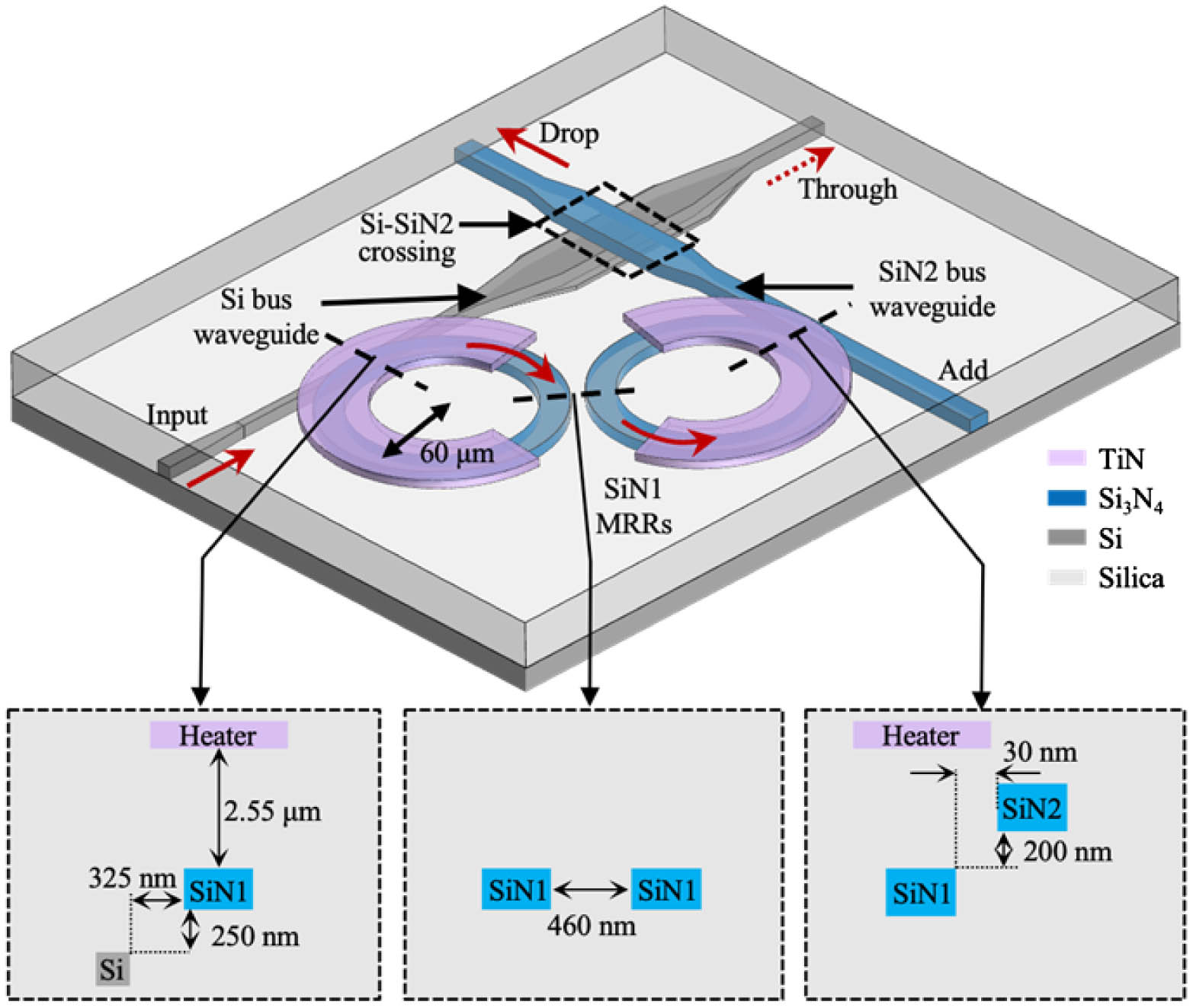
Figure 1 shows the structure of the proposed 3D integrated MRR SE, consisting of two MRRs vertically coupled with a 3D waveguide crossing. The silicon waveguide in the bottom layer (Si) underpasses the waveguide in the top layer (SiN2) at 90 deg, forming the 3D Si-SiN2 crossing. The dual-coupled MRRs are formed in the middle layer (SiN1). The thicknesses of the Si layer and the two layers are 220 nm and 400 nm, respectively. To balance the crossing loss and the interlayer transition loss, the layer spacings for Si-SiN1 and SiN1-SiN2 are designed as 250 nm and 200 nm, respectively. For the Si bus waveguide, the Si strip waveguide is transformed to a ridge waveguide at the crossing with a width of 2 μm to reduce the crossing loss. Similarly, the SiN2 bus waveguide at the crossing also expands to a width of 2 μm. With this design, the measured crossing losses of the Si and SiN2 waveguides are and at the 1563 nm wavelength, respectively, and the cross talk is less than [54].
Figure 1.Schematic of the MRR switch element. Solid red and dashed red arrows outline the transmission paths when the element works at the on-state and the off-state, respectively. The insets show the cross sections of the coupling regions.
The dual-coupled MRRs in the SiN1 layer have a waveguide width of 1 μm and a bending radius of 60 μm. Due to the large refractive index difference between the Si and the waveguides, the width of the Si bus waveguide is reduced to 260 nm via an adiabatic taper to achieve phase matching with the mode in the SiN1 MRR. The SiN2 bus waveguide is coupled to another SiN1 MRR. The lateral waveguide gaps between the Si bus waveguide and the SiN1 MRR, between the two SiN1 MRRs, and between the SiN2 bus waveguide and the SiN1 MRR, are designed to be 325 nm, 460 nm, and 30 nm, respectively. Cross-sectional structures of the three coupling sections mentioned above are shown in the insets of Fig. 1. It is noted that the lateral gap between SiN1 and SiN2 in the SE is only 30 nm. Since they are constructed by different layers, they can be patterned by 248 nm deep ultraviolet (DUV) lithography. We also analyzed the influence of gap variation on the switch performance, which shows good fabrication tolerance. The details are shown in Appendix B. Two titanium nitride (TiN) microheaters are placed above the SiN1 MRRs for TO switching operation. The MRR switch works at two switching states. At the off state, the input light bypasses the MRRs and goes through the Si waveguide. At the on state, the input light resonates with the MRRs, so it couples into the MRRs and outputs to the SiN2 waveguide at the drop-port.
Figure 2(a) shows the electric-field modal profile of the waveguide. The effective and group indices of the waveguide are 1.63 and 2.0, respectively. The designed free-spectral range (FSR) of the MRRs is 3.18 nm. Figure 2(b) shows the effective refractive index and the resonance wavelength changes with the waveguide width deviation for both Si and waveguides. We can see that the waveguide has a lower sensitivity; thus, the MRRs’ resonance wavelength variation (0.11 nm/nm) is much smaller than that of Si MRRs (0.55 nm/nm). Therefore, it implies the waveguide is more tolerant to fabrication imperfections.
Figure 2.(a) Electric-field intensity profile of the waveguide with cross-sectional dimensions of μμ. (b) Waveguide effective refractive index and MRR resonance wavelength changing with the waveguide width deviation for both Si and waveguides. The dimension of the Si waveguide is μμ.
Figure 3(a) shows the schematic of an crossbar switch with the proposed SE placed at each crossing point. We arranged the silicon waveguides horizontally and the waveguides vertically, thus deploying the waveguide crossings as 3D structures to reduce ILs and cross talk. Typically, only half of the ports in the crossbar switch are used, and the rest are redundant (marked with ). The idle ports in the crossbar structure can be used as another set of input and output ports of the synchronized switch and only need to be arranged according to a simple bidirectional path transmission. Based on the full port arrangement, when a path is established between ports and (, ), another path between ports and exists in the synchronization, which satisfies the condition of the two synchronous switches required for polarization diversity. Figure 3(b) is an example of the bidirectional path transmission; light from () is routed to () by turning on while the remaining SEs stay off.
Figure 3.(a) General port arrangement of the crossbar switch fabric. (b) Example of bidirectional path transmission. When is turned on, light from () is routed to ().
Figure 4(a) shows a micrograph of the switch chip fabricated by Advanced Micro Foundry (AMF). The chip footprint is . The switch consists of 64 dual-coupled MRR SEs, and the microscope image of SE is shown in Fig. 4(b). Waveguide interlayer couplers with bidirectional reverse tapers are used between the SiN2 waveguide outputs and the chip edge to achieve high-efficiency coupling between different waveguide layers by evanescent coupling. Near the 1560 nm wavelength, the IL for transition is about 0.15 dB [54]. Suspended Si edge couplers are placed at the chip edge for coupling light in and out; they are foundry PDK devices as illustrated in Fig. 4(c), and the coupling loss is about 3 dB per facet across C-band. Two 20-channel polarization maintaining (PM) fiber arrays (FAs) are butt-coupled to the chip edge. The switch chip is mounted on a metal base with all the electrical pads wire-bonded to a printed circuit board (PCB). The switch chip after optical and electrical packaging is shown in Fig. 4(d).
Figure 4.(a) Microscope image of the fabricated switch chip. (b) Microscope image of the switch element, with a TiN heater integrated on each SiN1 MRR. (c) Microscope image of the on-chip suspended edge couplers. (d) Photo of the switch chip after packaging.
Figures 5(a) and 5(b) show the measured transmission spectra of and () in the switch chip without active tuning. The wavelength range is from 1520 nm to 1580 nm, which covers the entire C-band and part of the L-band of optical communications. The insets in Figs. 5(a) and 5(b) show the zoom-in spectra near 1563 nm. The measured FSR of MRRs is 3.2 nm. The transmission spectra from to the eight output ports were also measured, and the magnified spectra around 1563 nm are shown in Fig. 5(c). The resonance wavelengths of all the MRRs are almost aligned, indicating that MRRs have excellent fabrication tolerance and negligible random phase errors. Therefore, the SEs are at the off-state without calibration. Only one SE needs to be turned on when a routing path is established. This reduces power consumption and simplifies the control system. One observes that the loss varies between different paths as shown in Figs. 5(a) and 5(b). It mainly comes from the coupling loss variation due to the fragile suspended edge couplers used in this chip, which is analyzed in Appendix A. As can be seen in Fig. 5(c), there are two asymmetric dips in the spectra from to . The strong coupling between the two MRRs causes resonance splitting, while backcoupling in the input coupler of the MRRs makes the resonance dip asymmetric [55].
Figure 5.(a) and (b) Through-transmission spectra of the crossbar switch. (c) Drop transmission spectra of eight output ports when light is launched from .
Next, we measured the transmission spectra of all the paths of this optical switch. The operating wavelength is set as 1563 nm, which requires the MRRs to be redshifted by about 1/2 FSR. In the measurement, a thermo-electric cooler (TEC) was turned on to stabilize the chip temperature. For the crossbar switch, there are two groups of routing paths transmitted in the opposite directions: and (, ), which have 64 paths in total for each group. It is unfortunate that the bonding wire connecting the electrode pad of to the PCB is open; this element cannot be tuned. The actual measured number of routing paths for each group is 63. Figures 6(a) and 6(b) show the overlaid transmission spectra of the routing paths in each group. The spectra show flattop passbands, which are preferred for broadband optical signal transmission. Figures 6(c) and 6(d) show the histogram of the extracted optical 3 dB bandwidth of each path. The measured bandwidths are in the range of 0.535–0.565 nm ( on average), which indicates good uniformity of the MRR SEs.
Figure 6.(a), (b) Transmission spectra of the routing paths of (a) and (b) . (c), (d) Histogram of the extracted optical 3-dB bandwidth for the paths of (c) and (d) (, ).
In each group, there are spectra for the leakage paths. The cross talk of a target path is defined as the ratio of the total leaked optical power from the other seven input ports to the optical power transmitted in the destination path. Figures 7(a) and 7(b) show the measured transmission and leakage spectra of routing paths and , respectively. In the measurement, only and were turned on separately. From the leakage spectra, we can observe that the resonance wavelengths of other MRR SEs are almost unchanged compared with the passive state, indicating the negligible thermal cross talk of the on-state SE. Near the operating wavelength of 1563 nm, the cross talk is about and for these two paths. These two states represent the worst and the best cross talk of the chip.
Figure 7.Transmission spectra of the target path and the leakages from other input ports for (a) the routing path and (b) the routing path . (c) Schematic of the ER definition of the on-state SE () and the off-state SE (). The through-port and drop-port transmissions of the on-state SE are plotted in solid lines, while those of the off-state SE are plotted in dash lines. Histograms of extracted (d) and (e) .
As can be seen, different input ports occupy different leakage optical power around the operating wavelength. The leakage is strongly related to the extinction ratio (ER) of SEs. The ERs of the on-state and the off-state SE are denoted as and . As illustrated in Fig. 7(c), and are defined as the absolute value of the loss difference between the operating wavelength and its nearby FSR/2 wavelength of the through-port and the drop-port, respectively. The extracted ERs of each SE are shown in Figs. 7(d) and 7(e). The variation of for all SEs is less than 2.76 dB, which indicates that the drop-port transmission responses of all SEs are nearly identical. The transmission response of the through-port near the operating wavelength is more sensitive to the waveguide coupling coefficients. The detailed calculation method is also shown in Appendix A.
The cross talk is mainly dependent on the SEs’ ER and also the number of off-state and on-state SEs in the routing and leakage paths. We assume all SEs have identical transmission responses and neglect the through-pass IL of the SEs to conveniently explain this cross talk variation in Figs. 7(a) and 7(b). For the routing path , the optical power from () is leaked to by the drop-port of the off-state . Therefore, the leakage of each input port is around . The cross talk, which is the sum of all the leakages, can be calculated as . On the contrary, for the routing path , the optical power from () is leaked to by the drop-port of the off-state and the through-port of the on-state , which is around . The cross talk is thus . Therefore, the cross talk for the routing path is lower than the path . As can be seen, the worst cross talk of the chip is essentially limited by of the SEs. To further improve the cross talk, we can reduce the coupling coefficient between MRRs. Consequently, the operation bandwidth will decrease accordingly.
C. Fiber-to-Fiber ILs
Figure 8 shows the extracted fiber-to-fiber (FtF) ILs of all 126 paths at the wavelength of 1563 nm, with the solid circles indicating the routing paths of and the hollow diamonds representing the routing paths of . In all paths, the minimum and the maximum ILs are 6.14 dB and 8.9 dB, respectively. And in another group of , the minimum and the maximum ILs are 6.69 dB and 11.7 dB, respectively. The loss variation between paths has no significant path length dependence. Typically, the IL is linearly proportional to the number of off-state SEs bypassed in the routing path. Due to the large random coupling loss variation for different input and output ports, we cannot accurately get the on-chip ILs of the chip.
Figure 8.Fiber-to-fiber ILs of all target ports at the wavelength of 1563 nm; 63 solid circles represent paths of (, ), and 63 hollow diamonds represent paths of .
To retrieve the actual on-chip ILs of the chip, we used the transfer matrix method to fit the IL of each SE. The details of the retrieving method and results are shown in Appendix A. The extracted average on-state and off-state ILs of the SEs are 0.37 dB and 0.021 dB, respectively. We also extracted the extra loss from the waveguide propagation and waveguide crossing loss in the routing paths. The extra losses in the horizontal Si waveguide transmission and the vertical SiN2 waveguide transmission are slightly different due to the different waveguide propagation losses of Si and . Based on the extracted loss, we can retrieve the on-chip ILs of the switch chip. Figure 9 shows the on-chip IL distribution. The on-chip ILs are 0.52–2.66 dB for the routing path of and 0.60–2.13 dB for the , considering the loss of the interlayer couplers. Therefore, we can confirm that the large variation of the FtF ILs is from the nonuniform coupling loss of the suspended Si edge couplers. In the future, we can improve the design of the edge coupler by using the layer on the multi-layer -on-SOI platform to expand the waveguide spot size without substrate undercut.
Figure 9.(a), (b) Heatmap of the on-chip ILs for path (a) and (b) .
As mentioned before, the crossbar architecture can also be configured as a non-duplicate polarization-diversity optical switch fabric with the assistance of PSRs. Figure 10(a) shows the structure of an non-duplicate polarization-diversity MRR optical switch consisting of the single all-port arranged crossbar switch chip and 16 PSRs. The inputs and outputs are labeled as 1, 2, …, 8, and , respectively. Each input/output port is connected with a PSR. The input PSRs are connected to the optical switch fabric from both the west and east sides, while the output PSRs are connected to the north and south sides of the switch. A path from the input port 5 to the output port is highlighted to show the operation principle. Input light with random polarization states from port 5 is divided into two paths by the PSR before entering the crossbar switch. The two outputs of the PSR are routed to the switch’s input port and reverse input port via Si connecting waveguides. The switch is designed for the TE mode. In the switch, the path with original TE-like polarization () is depicted by the solid orange line, while the path with original TM-like polarization () is depicted by the dotted orange line. By turning on, light from () is routed to (), as shown in Fig. 3(b). The switch’s output port and reverse output port are then connected to another PSR via connecting waveguides and interlayer couplers and output to port . Using this on-chip polarization-diversity scheme, both the Si and connecting waveguides can be embedded into the switch fabric with additional waveguide crossings in the crossbar optical switch, which is less than the crossing number () in the non-duplicate PILOSS switch [47]. Additionally, the 3D overpass structure has been employed at every crossing to efficiently reduce the loss and the cross talk.
Figure 10.(a) Schematic of a non-duplicate polarization-diversity switch. (b) Experimental verification for polarization diversity of the device under test (DUT).
Figure 10(b) shows the experimental setup of the non-duplicate polarization-diversity crossbar switch. As a proof-of-concept, we used fiber-based PBSs instead of the on-chip PSRs. It should be noted that various high-performance on-chip PSRs have been previously reported and can be readily integrated on the same chip [56–58]. Input light with random polarization states is divided into two beams by the PBS and connected to the switch chip with the PM FAs. By aligning the slow axis of the PBS outputs and the PM FAs, light coupled to the switch is adjusted to the TE-like polarization. The two optical signals are transmitted in opposite directions on the chip, coupled again to the PM FAs, and combined by another PBS.
B. Polarization-Diversity Verification
The polarization-dependent losses (PDLs) and DGDs for eight representative paths that pass through the diagonal SEs of the switch fabric are evaluated, as shown in Fig. 11(a). The polarization state of the input light was adjusted by a PC. The maximum difference of output optical power at different polarizations is the PDL. The maximum and minimum PDLs are 2.24 dB and 0.59 dB, respectively. Theoretically, the PDLs are related to the difference of the through-pass SE number in the two paths. The coupling loss variations, however, have a bigger effect in this test. In DGD experiments, the input optical pulses were generated by a pulse pattern generator (PPG, Keysight, N4951B) and a commercial intensity modulator. The output optical signal was received by a high-speed photodetector (u2t, XPDV2120R) and evaluated with a digital communications analyzer (DCA, Agilent DCA-X 86100D). The DGDs are the maximum time delay difference of the output pulses when adjusting the PC. The influence of two PBSs in the DGD measurement has been removed, while the length difference of the PM fibers after polarization splitting and before polarization combining has not been compensated. For the eight representative paths, the maximum, minimum, and average DGDs are 35.16 ps, 0.97 ps, and 17.46 ps, respectively. Figures 11(b) and 11(c) display the electrical signal responses for path with the maximum DGD and path with the minimum DGD, respectively. The DGDs are limited by the length difference between the PM FAs and the fiber-based PBSs, which can be further overcome by using on-chip PSRs.
Figure 11.(a) PDLs and DGDs for eight representative paths. (b), (c) Electrical signal responses for (b) path with the maximum DGD and (c) path with the minimum DGD.
We also performed a 100 Gb/s DP-QPSK signal transmission with our chip. The experimental setup is shown in Fig. 12. We used a tunable laser source to generate the continuous wave (CW) at 1563 nm and modulated it with a DP-IQ modulator to generate the DP-QPSK signal. The electrical driving signals based on four 25 Gb/s, pseudo-random bit sequence (PRBS) signals were generated by the PPG. Therefore, the data rate of the DP-QPSK optical signal is 100 Gb/s. The modulated optical signal was then amplified by an Er-doped fiber amplifier (EDFA) to compensate for the device loss. Since the MRR-based switches possess the filtering characteristics, we did add an extra bandpass filter to filter out the amplified spontaneous emission (ASE) noise generated by the EDFA. Finally, the optical signal was sent to an optical modulation analyzer (OMA, Keysight, N4392A) where the constellation diagram and the error vector magnitude (EVM) can be analyzed.
Figure 12.Experimental setup for 100 Gb/s DP-QPSK signal transmission over the polarization-diversity switch.
We first measured the back-to-back () optical signal with the OMA by bypassing the EDFA and the DUT. Figure 13 shows the measured DP-QPSK constellation diagrams. To compare the transmitted optical signals through the polarization-diversity optical switch, we tuned the received optical power to be the same as the by changing the gain power of the EDFA. We conducted signal transmission for the path: . As noted, the path has the largest PDL and DGD among the routing paths. As observed in the diagrams, the 100 Gb/s DP-QPSK signal passes through the optical switch with only slight degradation. Compared with the case, the EVM deterioration for both polarization states transmitted through the switch is within 1.5%. The results reveal that our polarization-diversity switch can transmit 100 Gb/s DP-QPSK data while maintaining high signal integrity.
Figure 13.Constellation diagrams in the back-to-back () configuration, and path of .
The above measurements reveal that the 3D dual-coupled MRR-based switch combining Si and waveguides has superior performances (see Table 1). The MRR-based optical switch has the lowest IL compared with the state-of-the-art MRR-based optical switch fabrics. Besides, our chip can realize non-duplicate polarization diversity for polarization-insensitive optical switching. The MRRs also have the advantages of large manufacturing tolerance and low temperature sensitivity, thus reducing the complexity of the switching control circuits. For an crossbar optical switch, the number of SEs that need to be turned on is N, linearly proportional to the port count. The average power consumption of a single SE is 363 mW, and the total power for the switch is . By introducing air trenches and substrate undercut, the switching power can be further reduced. On the other hand, due to the low through loss of the 3D MRR SEs ( from the SiN2 waveguide), this crossbar switch can be easily scaled up. For a switch, the maximum on-chip IL is 7.97 dB, and the path-dependent loss is less than 6.82 dB. The loss can be further reduced by optimizing the structure of the Si bus waveguide or replacing it with a waveguide to construct an optical switch structure with all waveguides. In this work, the maximum DGD is mainly caused by the PM fiber length difference, which can be avoided by using on-chip PSRs in the future. On-chip path length difference induced DGD of the crossbar switch also impacts the highest transmission baud rate when it scales to . We can put all the SEs closer to reduce the DGD and also use digital signal processing to compensate for DGD in digital-coherent transmission.
Characteristics Comparison of MRR-Based Photonic Switches
Refs.
Port Count
SE Struct.
Topology
Pol. Sensitivity
On-Chip IL (dB)
FtF IL (dB)
Bandwidth (GHz)
[16]
5th-order MRR
Crossbar
Sensitive
2–13.7
14–25.7
[22]
2nd-order MRR
Crossbar
Sensitive
6–14
19–27
100
[17]
1st-order MRR
Switch & select
Sensitive
1.8–20.4
12.8–31.4
24
[20]
2nd-order MRR
Butterfly
Sensitive
55
[21]
Dual-MRR
Omega
Sensitive
4.4–9.6
11.6–16.8
55
[46]
1st-order MRR
Switch & select
Insensitive
4–7.8
14.8–18.6
50
This work
2nd-order MRR
Crossbar
Insensitive
0.52–2.66
6.14–8.9
6. CONCLUSION
We have demonstrated the first low-loss and large-bandwidth MRR crossbar switch on a multi-layer -on-SOI platform. By combining the advantages of silicon and nitride materials, our switch chip outperforms the state-of-the-art MRR switches in terms of loss, control complexity, and polarization insensitivity. The 3D MRR-based switch possesses uniform switching states and negligible waveguide crossing loss. The measurements show that the 3D MRRs have a low through loss of for the vertical SiN2 waveguide transmission direction, effectively reducing the path-dependent IL of the crossbar switch and making it highly scalable. The on-chip ILs are only 0.52–2.66 dB, the lowest among all reported results up to now for microring-based optical switches. The 3 dB optical bandwidth of the fabricated switch is , and the cross talk is . In addition, the bidirectional transmission characteristics of the crossbar topology have been used to implement a non-duplicate polarization-diversity optical switch. The optical signal transmission was successfully verified by using a 100 Gb/s DP-QPSK signal. Based on these features, we believe that 3D MRR-based switches hold great promise for future applications in high-performance networks. Moreover, the 3D integration, which fully exploits the advantages of both silicon and nitride materials, opens up a new way to achieve high-density photonic integration.
Acknowledgment
Acknowledgment. The authors thank Dr. Xianshu Luo for his helpful suggestions on chip design and fabrication.
APPENDIX A: EXTRACTION OF THE ON-CHIP ILs AND ERs
We used the transfer matrix method to fit the IL of each SE. Each (, ) in the crossbar switch has two groups of transmission spectra when it is turned on: and . The electric-field transfer expressions at the drop-ports are the same, as follows: where and (, 2, 3) are the coupling and the transmission coefficients of the three coupling sections in the SE (assuming lossless coupling, ), and is the round trip loss factor. is the round trip phase change of the two MRRs, assuming the two MRRs have the same phase, where . and are the effective refractive index and the perimeter of the MRRs, and is the applied phase by the phase shifters. The transfer functions of the through-ports for these two groups are slightly different, as shown below:
To fit with the experimental transmission spectra, the optical power transmission expressions of the drop-ports are as follows: where C and are the loss coefficients, including the coupling loss and the loss from the bypass SEs. Using the lsqcurvefit function in the MATLAB toolbox, we obtained the parameters for each SE. Figure 14 shows the curve-fitting results of eight representative diagonal SEs of the switch fabric. All the fitting curves are consistent with the measured transmission spectra. The square of the residual norm fitted by all SEs is less than 0.01, indicating that all SEs are well fitted. From the fitted results, we find that the coupling coefficient between the two MRRs of and () is relatively less than those of the other SEs. It can be seen from the representative fitted results of and in Figs. 14(d) and 14(e).
Figure 14.Curve fitting results of eight representative diagonal SEs of the switch fabric. The solid blue and red lines represent the measured transmission spectra of and (), respectively. The dashed yellow and purple lines are the correspondingly fitted curves.
Figure 15.(a), (c), (e) Heatmaps and (b), (d), (f) corresponding histograms of extracted (a), (b) on-state loss, (c), (d) off-state loss from the Si waveguide direction, and (e), (f) off-state loss from the SiN2 waveguide direction of all the SEs in the chip.
APPENDIX B: TOLERANCE ANALYSIS OF THE WAVEGUIDE GAP
We note that the separation gap between SiN1 and SiN2 of the SEs is only 30 nm. As mentioned, it can be patterned by 248 nm deep ultra-violet (DUV) lithography. However, the alignment precision of the two waveguide layers also influences the fabricated gap. We simulated the waveguide coupling coefficient at 1560 nm versus waveguide gap deviation, as shown in Fig. 17(a). Figure 17(b) shows the change of SE loss with the waveguide gap deviation. As the waveguide gap varies within , the off- and on-state loss of the SE varies within 0.01 dB and 0.1 dB, respectively. Figure 17(c) shows the effect on the of SE, which varies by less than 2 dB. Therefore, the waveguide gap has good fabrication tolerance.
Figure 17.(a) Interlayer waveguide coupling coefficient, (b) on- and off-state IL and (c) of the MRR SE changing with the deviation of the SiN2 bus waveguide and the SiN1 MRR gap.
[3] H. Ballani, P. Costa, R. Behrendt, D. Cletheroe, I. Haller, K. Jozwik, F. Karinou, S. Lange, K. Shi, B. Thomsen, H. Williams. Sirius: a flat datacenter network with nanosecond optical switching. Annual Conference of the ACM Special Interest Group on Data Communication on the Applications, Technologies, Architectures, and Protocols for Computer Communication, 782-797(2020).
[13] W. Gao, X. Li, L. Lu, J. Chen, L. Zhou. Broadband, low-crosstalk and power-efficient 32 × 32 optical switch on a dual-layer Si3N4-on-SOI platform. Optical Fiber Communications Conference and Exhibition (OFC), W4B.4(2022).
[28] J. C. C. Mak, W. D. Sacher, J. C. Mikkelsen, T. Xue, Z. Yong, J. K. S. Poon. Automated calibration of high-order microring filters. CLEO: 2015, SW1N.2(2015).
[29] A. Gazman, C. Browning, Z. Zhu, L. R. Barry, K. Bergman. Automated thermal stabilization of cascaded silicon photonic ring resonators for reconfigurable WDM applications. European Conference on Optical Communication (ECOC), 1-3(2017).
[32] M. Hattink, L. Y. Dai, Z. Zhu, K. Bergman. Streamlined architecture for thermal control and stabilization of cascaded DWDM micro-ring filters bus. Optical Fiber Communication Conference (OFC), W2A.2(2022).
[35] Q. Zhu, S. An, R. Cao, Y. Ling, Y. Su. Fast and wide-range wavelength locking based on a two-layer neural network in a silicon microring switch. Optical Fiber Communication Conference (OFC), W1E.1(2019).
[45] H. Yang, Q. Cheng, R. Chen, K. Bergman. Polarization-diversity microring-based optical switch fabric in a switch-and-select architecture. Optical Fiber Communications Conference and Exhibition (OFC), Th3B.2(2020).
[50] W. Xu, Y. Guo, X. Li, C. Liu, L. Lu, J. Chen, L. Zhou. Fully integrated solid-state LiDAR transmitter on a multi-layer silicon-nitride-on-silicon photonic platform. Optical Fiber Communication Conference (OFC), Th1E.4(2022).
[54] X. Li, W. Gao, L. Lu, J. Chen, L. Zhou. 8 × 8 microring optical switch on a dual-layer Si3N4-on-SOI platform. Asia Communications and Photonics Conference, T1I.1(2021).
[58] W. D. Sacher, T. Barwicz, J. K. S. Poon. Silicon-on-insulator polarization splitter-rotator based on TM0-TE1 mode conversion in a bi-level taper. CLEO Science and Innovations, CTu3F.3(2013).