• Chinese Optics Letters
  • Vol. 15, Issue 6, 062401 (2017)
Qi Wang1, Li Zhang1, Xin Wang1, Haiyan Quan1, Zhanguo Chen1、*, Jihong Zhao1, Xiuhuan Liu2, Lixin Hou3, Yanjun Gao1, Gang Jia1, and Shaowu Chen4
Author Affiliations
  • 1State Key Laboratory on Integrated Optoelectronics, College of Electronic Science and Engineering, Jilin University, Changchun 130012, China
  • 2College of Communication Engineering, Jilin University, Changchun 130012, China
  • 3College of Information Technology, Jilin Agricultural University, Changchun 130118, China
  • 4State Key Laboratory on Integrated Optoelectronics, Institute of Semiconductors, Chinese Academy of Sciences, Beijing 100083, China
  • show less
    DOI: 10.3788/COL201715.062401 Cite this Article Set citation alerts
    Qi Wang, Li Zhang, Xin Wang, Haiyan Quan, Zhanguo Chen, Jihong Zhao, Xiuhuan Liu, Lixin Hou, Yanjun Gao, Gang Jia, Shaowu Chen. Optical rectification and Pockels effect as a method to detect the properties of Si surfaces[J]. Chinese Optics Letters, 2017, 15(6): 062401 Copy Citation Text show less
    Orientations of the Si(110) crystal.
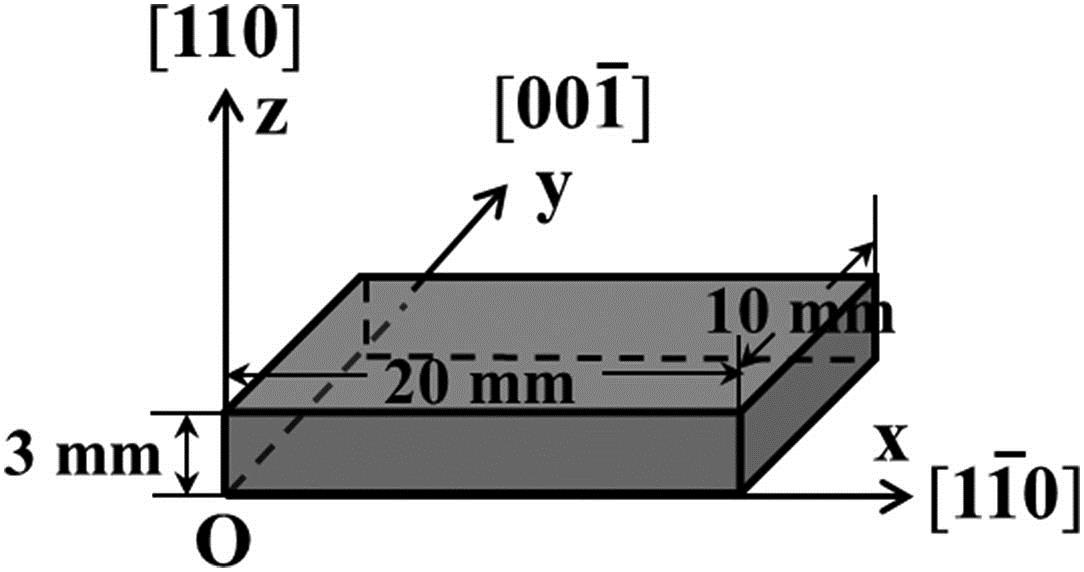
    Fig. 1. Orientations of the Si(110) crystal.
    Anisotropy of EFI OR in the Si(110) surface layers.
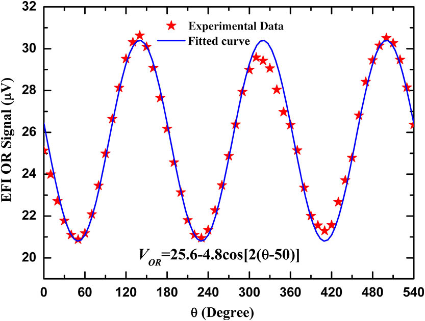
    Fig. 2. Anisotropy of EFI OR in the Si(110) surface layers.
    Relative shift between the sample and the laser spot.
    Fig. 3. Relative shift between the sample and the laser spot.
    Distribution of EFI OR signals along the depth direction in the Si(110) crystal. The experimental results (a) before and (b) after reversing the two {110} surfaces of the Si crystal are in good accordance. The blue solid lines are the theoretical simulation curves.
    Fig. 4. Distribution of EFI OR signals along the depth direction in the Si(110) crystal. The experimental results (a) before and (b) after reversing the two {110} surfaces of the Si crystal are in good accordance. The blue solid lines are the theoretical simulation curves.
    EFI PE signals in (a) the No. 1 surface layer and (b) the No. 2 surface layer of the Si(110) crystal.
    Fig. 5. EFI PE signals in (a) the No. 1 surface layer and (b) the No. 2 surface layer of the Si(110) crystal.
    (a) Band structure of the Si(110) crystal after contact with the Al electrodes. (b) Distribution of the built-in electric field in the SCR of the Si surface layers. The dashed lines represent the boundary of the SCR.
    Fig. 6. (a) Band structure of the Si(110) crystal after contact with the Al electrodes. (b) Distribution of the built-in electric field in the SCR of the Si surface layers. The dashed lines represent the boundary of the SCR.
    Intensity distribution of the Gaussian beam on the z axis and the overlap of the Gaussian beam and the SCR. The dashed lines are the boundaries of the SCR. The shadow area is the tiny integration zone of z to z+dz, where the laser beam and the SCR overlap. (a) Overlap of the first surface layer and the Gaussian beam. (b) Overlap of the second surface layer and the Gaussian beam.
    Fig. 7. Intensity distribution of the Gaussian beam on the z axis and the overlap of the Gaussian beam and the SCR. The dashed lines are the boundaries of the SCR. The shadow area is the tiny integration zone of ztoz+dz, where the laser beam and the SCR overlap. (a) Overlap of the first surface layer and the Gaussian beam. (b) Overlap of the second surface layer and the Gaussian beam.
    Qi Wang, Li Zhang, Xin Wang, Haiyan Quan, Zhanguo Chen, Jihong Zhao, Xiuhuan Liu, Lixin Hou, Yanjun Gao, Gang Jia, Shaowu Chen. Optical rectification and Pockels effect as a method to detect the properties of Si surfaces[J]. Chinese Optics Letters, 2017, 15(6): 062401
    Download Citation