Qi Wang, Li Zhang, Xin Wang, Haiyan Quan, Zhanguo Chen, Jihong Zhao, Xiuhuan Liu, Lixin Hou, Yanjun Gao, Gang Jia, Shaowu Chen, "Optical rectification and Pockels effect as a method to detect the properties of Si surfaces," Chin. Opt. Lett. 15, 062401 (2017)
Copy Citation Text
The depth profile of electric-field-induced (EFI) optical rectification (OR) and EFI Pockels effect (PE) in a Si(110) crystal are investigated. The results show that EFI OR and PE signals are very sensitive to the electric field strength in the surface layers of the Si crystal. Theoretical formulas that include the electric field parameters and the widths of the space-charge region are presented and agreed very well with the experimental results. The experiments and simulations indicate that EFI OR and PE are potential methods for researching the surface/interface properties along the depth direction in centrosymmetric crystals such as Si.
Second-order nonlinear optical effects, such as optical rectification (OR) and the Pockels effect (PE), have important applications in the microelectronics industry. OR has been used for terahertz generation[1,2], which is promising in photoelectric communication and imaging. The PE not only is a standard mechanism used in modulation devices, but also has been used for the measurement of electric signals[3,4].
In centrosymmetric materials, such as Si and Ge, OR and the PE are theoretically forbidden according to the electric-dipole approximation. However, an asymmetric stress or an electric field can break the symmetry and induce various second-order nonlinear optical effects[5]. Stress-induced PE and second-harmonic generation (SHG) have been found recently in strained Si[6–10]. Local electric-field-induced (EFI) second-order nonlinear optical effects, such as EFI SHG[11,12], EFI PE, and EFI OR[13–15], were observed. EFI SHG and EFI second-harmonic spectroscopy have been widely used for characterization of interfaces in metal–oxide–semiconductor (MOS) devices[16–24]. In these investigations, researchers mainly focused on Si(111) or Si(001) surfaces, and there have been very few papers on the nonlinear optical effects of Si(110) surfaces. Furthermore, researchers usually applied in-plane scanning to characterize the surfaces or interfaces, especially for SHG detection[25,26]. It is well known that space-charge regions (SCRs) often exist in the surface/interface layers of Si devices. The width of the SCR and the distribution of a nonuniform electric field in the SCR are closely related to the surface/interface properties, such as surface/interface states and surface/interface charges. Nevertheless, the in-plane scanning method cannot reveal the detailed characteristics of SCRs.
In this Letter, we investigated EFI OR and the EFI PE in Si(110) surface layers. In particular, we measured and analyzed the depth profile of the EFI OR, namely, the distribution of EFI OR signals along the thickness direction of the Si(110) crystals. The EFI OR depends on the electric field and the width of the SCRs, according to the theoretical simulations. Experimental results show that EFI OR and the EFI PE are very sensitive to the surface properties and are potential methods for characterizing the surfaces of Si or other centrosymmetric materials.
Sign up for Chinese Optics Letters TOC. Get the latest issue of Chinese Optics Letters delivered right to you!Sign up now
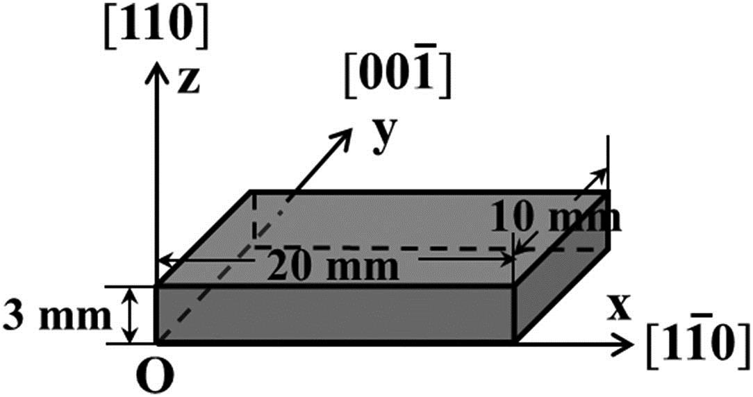
The sample is a lightly doped -type Si(110) crystal with a resistivity that is over , as shown in Fig. 1. The side surfaces of the crystal are the , , and (110) planes. The crystal was mechanically polished before experiments.
The same measurement system that was used in Refs. [18–20] for the EFI OR also was used in this work. If the azimuth with respect to the axis of the linearly polarized light is , the dc polarization along the axis (namely the [110] orientation) can be expressed as where is the permittivity of Si; is the optical field of the probing beam; and, and are components of the effective second-order susceptibility tensor in the Si(110) surface layers, which correspond to the product of the built-in electric field and the third-order susceptibility of Si[27] and can be written as
In Fig. 2, the measured EFI OR signals show a cosine dependence on , which agrees well with Eq. (1). It is noted that the EFI OR signals have a considerable background and an initial phase. But, this does not affect the nature of the experimental results. The background is probably due to the fact that and are close, so their sum is much larger than their difference. According to the fitted function in Fig. 2, the ratio of is calculated to be about 1.46. The initial phase is due to the initial azimuth between the polarizer and the half-wave plate.
Figure 2.Anisotropy of EFI OR in the Si(110) surface layers.
We further investigated the depth profile of EFI OR in the Si(110) crystal. The azimuth, , remained constant in the experiments. Measurements began from a position where the laser beam was far away from the sample. The laser was fixed, and the Si sample moved toward the laser beam along the axis with a step length of 20 μm. The laser beam propagated, in turn, through one surface layer, the body, and the other surface layer of the crystal and then finally was away from the sample. The relative shift is shown in Fig. 3. The solid line arrow stands for the movement direction of the sample, while the dashed-line arrows represent the relative movement of the laser beam. Thus, we could obtain the depth profile of the EFI OR signals.
Figure 3.Relative shift between the sample and the laser spot.
The normalized EFI OR signals are shown in Fig. 4. The center of the laser spot is always defined as the origin of the coordinate. Usually, the width of the SCR is much smaller than the waist of the laser beam, which is 1 mm, since the laser beam is not focused. The EFI OR signals should have maxima when the two interfaces between the Si crystal and aluminum electrodes overlap the center of the laser spot. In Fig. 4(a), there are two EFI OR peaks whose separation distance is 2920 μm, which just corresponds to the thickness of the sample after polishing. However, the intensities of the two peaks are much different. The first EFI OR peak is about 2.1 times as large as the second one.
Figure 4.Distribution of EFI OR signals along the depth direction in the Si(110) crystal. The experimental results (a) before and (b) after reversing the two {110} surfaces of the Si crystal are in good accordance. The blue solid lines are the theoretical simulation curves.
In order to eliminate the possibility of measurement error, we reversed the two surfaces of the Si crystal and repeated the experiment. The EFI OR signal at the No. 1 surface is still about 2.1 times as large as that at the No. 2 surface, as shown in Fig. 4(b). The distance between the two peaks is 2940 μm, which is in good accordance with the results in Fig. 4(a). According to Fig. 4, the EFI OR signals decrease gradually as the laser spot moves away from the surface layers because of the reduction in optical power irradiating through the SCR. Inside the Si crystal, the EFI OR signals almost disappear since there is little optical power through the SCR, and the residual signals can be attributed mainly to measurement errors, such as nonvertical incidence or diffusion of the probing beam.
It must be pointed out that the natural discontinuity of the lattice at surfaces and the bulk quadrupole should also contribute to the OR signals. The contribution of the bulk quadrupole is usually too weak to be considered. The contribution from the lattice discontinuity should give rise to comparable OR signals at the two Si(110) surfaces. However, as we can see, the two measured OR peaks are quite different. Moreover, the contribution from the surface discontinuity usually takes place in several atom layers, while the SCR usually includes thousands of atom layers. So, the measured OR signals should mainly result from the EFI second-order nonlinearity in the SCR, instead of surface discontinuity.
OR is the inverse effect of the PE. Since EFI OR can reveal the surface properties of Si, the EFI PE should also be sensitive to the surface properties. Thus, we carried out the measurement of the EFI PE using the same Si(110) crystal. The Si(110) crystal was sandwiched by two metal electrodes, and an insulating layer was added between one electrode and the crystal to prevent carriers from injecting. An AC modulation voltage was applied with a low-frequency signal generator. The laser beam always propagated through the Si(110) surface layer, which was in contact with the insulating layer.
First, we contacted the No. 1 surface of the crystal with the insulating layer, adjusted the relative position of the sample with respect to the probing beam and obtained the maximum EFI PE signal in this surface layer. Then, we reversed the crystal, contacting the No. 2 surface with the insulating layer, and repeated the experiment. The measured electro-optic (EO) signals are shown in Fig. 5. They are perfect linear modulations. The slope of the fitted line in Fig. 5(a) is 1.8 times that in Fig. 5(b). It is clear that the second-order nonlinearity in the No. 1 surface layer is much stronger than that in the No. 2 surface layer. The EFI PE results also reveal that the properties of the two (110) surface layers, as well as the built-in electric field and the effective second-order nonlinear susceptibilities, are different.
Figure 5.EFI PE signals in (a) the No. 1 surface layer and (b) the No. 2 surface layer of the Si(110) crystal.
A theoretical analysis is taken into account. The donor density of the Si sample is about , so the Femi level, , is about 0.15 eV above the intrinsic Femi level, . The electron affinity of Si is about 4.05 eV; thus, the work function of the Si(110) sample is about 4.46 eV, larger than that of Al electrodes (). Given that there are surface or interface states at Si(110) surfaces, and represent the neutral levels of the surface state and are lower than the Femi levels of the Si sample and the Al electrodes; is the thickness of the interfacial layer, which is only several angstroms and transparent to electrons[28]. Thus, the acceptor interface states will accept electrons from the surface layers of Si and the Al electrodes, and the energy bands of the Si surface layers bend upward. Figure 6(a) is the band structure of the Si(110) crystal in contact with the Al electrodes. Since the carriers are depleted in the surface layers, the carrier effects can be omitted in our experiments[29]. The built-in electric field in the Si crystal is sketched in Fig. 6(b) and is usually a linear function of the depth coordinate according to the depletion layer approximation. decreases from the maxima at the surfaces to zero inside the Si crystal. Provided that the widths of the SCRs in the two surface layers of the Si sample are and , that the coordinate of the first surface of the crystal is , and that the thickness of the crystal is , then the function for the built-in electric field can be written as where and are the maxima of at the two surfaces, and [24]. Usually, the probing beam is a Gaussian beam, whose intensity at the XOZ plane can be expressed as where is the total power of the laser beam, and is the waist radius of the laser beam. The intensity of the laser beam along the axis is shown in Fig. 7. The EFI OR signal can only be detected in the region where the laser beam and the SCR overlapped.
Figure 6.(a) Band structure of the Si(110) crystal after contact with the Al electrodes. (b) Distribution of the built-in electric field in the SCR of the Si surface layers. The dashed lines represent the boundary of the SCR.
Figure 7.Intensity distribution of the Gaussian beam on the axis and the overlap of the Gaussian beam and the SCR. The dashed lines are the boundaries of the SCR. The shadow area is the tiny integration zone of , where the laser beam and the SCR overlap. (a) Overlap of the first surface layer and the Gaussian beam. (b) Overlap of the second surface layer and the Gaussian beam.
The measured OR signals, , should be proportional to the product of the light intensity and the built-in electric field, which can be expressed as Substituting Eqs. (3) and (4) into Eq. (5), the final integration of ) can be written as
In accordance with Eqs. (3)–(6), a simulation was carried out with the MathCAD software. By adjusting the values of parameters, such as the maximum intensities of the built-in electric fields, and , and the widths of the SCRs, and , we could obtain the values of . Then, the simulated OR signals, , were normalized with the value of ) in Fig. 4(a) or in Fig. 4(b).
Note that the obtained EFI OR signals result from a superposition contribution of the built-in electric field in SCR and the optical field. The width of the SCR is proportional to the maximum electric field intensity. The smaller the built-in electric field intensity is, the smaller the overlapping area is. The EFI OR signals are proportional to an overlap integral such as Eq. (6). As deduced from the simulations, when the ratios of and are both assigned to be 1.45/1, the blue simulation curves shown in Fig. 4 agree well with the experiments. According to Eqs. (2) and (3), the effective second-order nonlinear susceptibilities in the Si(110) surface layers take on a linear distribution, and the maximum at the No. 1 surface is 1.45 times as large as that at the No. 2 surface. The small differences between the experimental and simulation results are attributed to measurement error, the nonideality of the Gaussian beam, and some residual absorption by impurities, defects, or interfaces states. In the experiments, the wavelength of laser beam is much larger than the intrinsic absorption edge of Si, and the laser power is low enough to ignore two-photon absorption, so the contribution of photon-generated carriers to the measured OR signals can be neglected.
In conclusion, we investigate the distribution of the EFI OR along the depth direction in Si(110) crystals. It is verified that EFI OR signals are sensitive to the properties of surfaces, especially the built-in electric fields, which is also verified by the experiment of EFI PE. The EFI OR method is able to distinguish the difference of the electric fields. Moreover, we bring up the theoretical formulas including the parameters of the electric field strength and the width of the SCR to simulate the EFI OR signals, and the simulation results agree well with the experiments. The results indicate that the EFI OR should be a potential nondestructive method to investigate and compare the surface/interface properties of centrosymmetric crystals, such as the distributions of electric fields along the depth direction.
Qi Wang, Li Zhang, Xin Wang, Haiyan Quan, Zhanguo Chen, Jihong Zhao, Xiuhuan Liu, Lixin Hou, Yanjun Gao, Gang Jia, Shaowu Chen, "Optical rectification and Pockels effect as a method to detect the properties of Si surfaces," Chin. Opt. Lett. 15, 062401 (2017)