• Photonics Research
  • Vol. 6, Issue 1, 37 (2018)
Yusheng Bian1、†, Qiang Ren1、2、†, Lei Kang1, Taiwei Yue1, Pingjuan L. Werner1, and Douglas H. Werner1、*
Author Affiliations
  • 1Department of Electrical Engineering, The Pennsylvania State University, University Park, Pennsylvania 16802, USA
  • 2School of Electronics and Information Engineering, Beihang University, Beijing 100191, China
  • show less
    DOI: 10.1364/PRJ.6.000037 Cite this Article Set citation alerts
    Yusheng Bian, Qiang Ren, Lei Kang, Taiwei Yue, Pingjuan L. Werner, Douglas H. Werner. Deep-subwavelength light transmission in hybrid nanowire-loaded silicon nano-rib waveguides[J]. Photonics Research, 2018, 6(1): 37 Copy Citation Text show less
    Hybrid nanowire-loaded silicon nano-rib waveguide. (a) Schematic of the 3D geometry. (b) Cross section of the configuration within the x-y plane. The hybrid waveguide comprises a silver nanowire (with a radius of r) located above a silicon nano-rib structure on a silica substrate. An additional silica buffer layer (with a height of h) is sandwiched between the nanowire and the silicon slab, which also determines the gap size (i.e., g=h). The height of the silicon waveguide is H, and the rib width is w. The nanowire is positioned at the center (along the x axis) with respect to the silicon nano-rib.
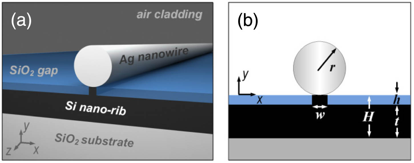
    Fig. 1. Hybrid nanowire-loaded silicon nano-rib waveguide. (a) Schematic of the 3D geometry. (b) Cross section of the configuration within the x-y plane. The hybrid waveguide comprises a silver nanowire (with a radius of r) located above a silicon nano-rib structure on a silica substrate. An additional silica buffer layer (with a height of h) is sandwiched between the nanowire and the silicon slab, which also determines the gap size (i.e., g=h). The height of the silicon waveguide is H, and the rib width is w. The nanowire is positioned at the center (along the x axis) with respect to the silicon nano-rib.
    Normalized electric field distributions of the fundamental hybrid plasmonic mode supported by a typical hybrid nanowire-loaded nano-rib waveguide. The geometric parameters of the waveguide are w=10 nm, h=g=5 nm, r=75 nm, and t=60 nm. (a) 2D electric field profile in the x-y plane. 1D electric field plots along the (b) x and (c) y directions, respectively. The 1D field profiles are evaluated at the bottom corner of the silver nanowire.
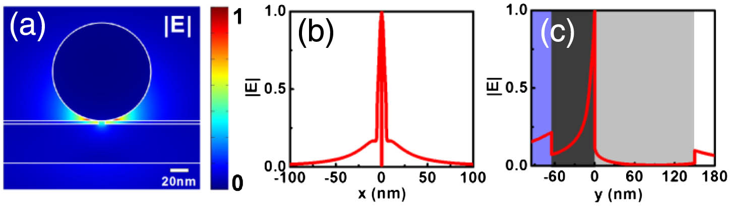
    Fig. 2. Normalized electric field distributions of the fundamental hybrid plasmonic mode supported by a typical hybrid nanowire-loaded nano-rib waveguide. The geometric parameters of the waveguide are w=10  nm, h=g=5  nm, r=75  nm, and t=60  nm. (a) 2D electric field profile in the x-y plane. 1D electric field plots along the (b) x and (c) y directions, respectively. The 1D field profiles are evaluated at the bottom corner of the silver nanowire.
    Dependence of modal properties on the radius of the silver nanowire for a silicon slab with different thicknesses (w=10 nm, h=5 nm): (a) modal effective index (neff); (b) propagation length (L), inset showing schematically the considered hybrid gap region in the study; (c) normalized mode area (Aeff/A0); (d) confinement factor in the hybrid gap (Γgap); (e) confinement factor inside the silicon region (ΓSi); (f) FoM. The dashed black line in (a) corresponds to the refractive index of the SiO2 substrate (ns=1.444).
    Fig. 3. Dependence of modal properties on the radius of the silver nanowire for a silicon slab with different thicknesses (w=10  nm, h=5  nm): (a) modal effective index (neff); (b) propagation length (L), inset showing schematically the considered hybrid gap region in the study; (c) normalized mode area (Aeff/A0); (d) confinement factor in the hybrid gap (Γgap); (e) confinement factor inside the silicon region (ΓSi); (f) FoM. The dashed black line in (a) corresponds to the refractive index of the SiO2 substrate (ns=1.444).
    Dependence of the modal properties on the size of the silicon nano-rib (r=50 nm, t=40 nm): (a) modal effective index (neff); (b) propagation length (L); (c) normalized mode area (Aeff/A0); (d) confinement factor inside the hybrid gap (Γgap); (e) confinement factor within the silicon region (ΓSi); (f) FoM. The dashed black line in (a) represents the refractive index of the SiO2 substrate (ns=1.444). The inset in (d) shows schematically the hybrid gap region considered in the study.
    Fig. 4. Dependence of the modal properties on the size of the silicon nano-rib (r=50  nm, t=40  nm): (a) modal effective index (neff); (b) propagation length (L); (c) normalized mode area (Aeff/A0); (d) confinement factor inside the hybrid gap (Γgap); (e) confinement factor within the silicon region (ΓSi); (f) FoM. The dashed black line in (a) represents the refractive index of the SiO2 substrate (ns=1.444). The inset in (d) shows schematically the hybrid gap region considered in the study.
    Dependence of the hybrid mode’s properties on lateral misalignments (the waveguide dimensions are r=50 nm, t=40 nm, w=10 nm, and h=5 nm): (a) modal effective index (neff); (b) propagation length (L); (c) normalized mode area (Aeff/A0); (d) confinement factor in the hybrid gap (Γgap); (e) confinement factor inside the silicon region (ΓSi); (f) FoM. The dashed black line in (a) corresponds to the refractive index of the SiO2 substrate (ns=1.444). The inset in (c) displays the electric field profile for the fundamental mode in a hybrid waveguide when Δx=5 nm. The inset in (d) shows the 2D schematic of a hybrid nanowire-loaded nano-rib waveguide with a laterally displaced silver nanowire. The deviation of the nanowire with respect to the silicon nano-rib is denoted as Δx.
    Fig. 5. Dependence of the hybrid mode’s properties on lateral misalignments (the waveguide dimensions are r=50  nm, t=40  nm, w=10  nm, and h=5  nm): (a) modal effective index (neff); (b) propagation length (L); (c) normalized mode area (Aeff/A0); (d) confinement factor in the hybrid gap (Γgap); (e) confinement factor inside the silicon region (ΓSi); (f) FoM. The dashed black line in (a) corresponds to the refractive index of the SiO2 substrate (ns=1.444). The inset in (c) displays the electric field profile for the fundamental mode in a hybrid waveguide when Δx=5  nm. The inset in (d) shows the 2D schematic of a hybrid nanowire-loaded nano-rib waveguide with a laterally displaced silver nanowire. The deviation of the nanowire with respect to the silicon nano-rib is denoted as Δx.
    Dependence of the hybrid mode’s properties on Δw (the waveguide dimensions are r=50 nm, t=40 nm, w=10 nm, and h=5 nm): (a) modal effective index (neff); (b) propagation length (L); (c) normalized mode area (Aeff/A0); (d) confinement factor in the hybrid gap (Γgap); (e) confinement factor inside the silicon region (ΓSi); (f) FoM. The dashed black line in (a) corresponds to the refractive index of the SiO2 substrate (ns=1.444). The inset in (b) shows the 2D schematic of a hybrid nanowire-loaded nano-rib waveguide with a nonideal silicon nano-rib. The variation in the nano-rib width is denoted as Δw.
    Fig. 6. Dependence of the hybrid mode’s properties on Δw (the waveguide dimensions are r=50  nm, t=40  nm, w=10  nm, and h=5  nm): (a) modal effective index (neff); (b) propagation length (L); (c) normalized mode area (Aeff/A0); (d) confinement factor in the hybrid gap (Γgap); (e) confinement factor inside the silicon region (ΓSi); (f) FoM. The dashed black line in (a) corresponds to the refractive index of the SiO2 substrate (ns=1.444). The inset in (b) shows the 2D schematic of a hybrid nanowire-loaded nano-rib waveguide with a nonideal silicon nano-rib. The variation in the nano-rib width is denoted as Δw.
    (a), (b) Parametric plots of normalized mode area (Aeff/A0) versus normalized propagation length (L/λ). (a) The curves for hybrid nanowire-loaded nano-rib waveguides are obtained by replotting the results in Figs. 3(b) and 3(c). For the hybrid nanowire-loaded nano-rib waveguide and metallic nanowire waveguide, a trajectory corresponds to a range of nanowire radius: r=[10,80] nm. Arrows indicate increasing the size of the nanowire. The HPW comprises a silicon nanowire embedded in silica near a silver substrate. Its dimensions are r=100 nm, g=5 nm. (b) The curves for hybrid nanowire-loaded nano-rib waveguides are obtained by replotting the results in Figs. 4(b) and 4(c). For the hybrid nanowire-loaded nano-rib waveguide and HPW, a trajectory corresponds to a range of nano-rib height (gap size): h=g=[2,20] nm. Arrows indicate increasing h(g). The radii of the HPW and the metallic nanowire waveguide are 100 and 50 nm, respectively. NW, nanowire.
    Fig. 7. (a), (b) Parametric plots of normalized mode area (Aeff/A0) versus normalized propagation length (L/λ). (a) The curves for hybrid nanowire-loaded nano-rib waveguides are obtained by replotting the results in Figs. 3(b) and 3(c). For the hybrid nanowire-loaded nano-rib waveguide and metallic nanowire waveguide, a trajectory corresponds to a range of nanowire radius: r=[10,80]nm. Arrows indicate increasing the size of the nanowire. The HPW comprises a silicon nanowire embedded in silica near a silver substrate. Its dimensions are r=100  nm, g=5  nm. (b) The curves for hybrid nanowire-loaded nano-rib waveguides are obtained by replotting the results in Figs. 4(b) and 4(c). For the hybrid nanowire-loaded nano-rib waveguide and HPW, a trajectory corresponds to a range of nano-rib height (gap size): h=g=[2,20]nm. Arrows indicate increasing h(g). The radii of the HPW and the metallic nanowire waveguide are 100 and 50 nm, respectively. NW, nanowire.
    Cross talk analysis for the proposed hybrid nanowire-loaded nano-rib waveguides, and performance comparison with metallic nanowire-loaded SOI waveguides and nanowire waveguides. (a) 3D schematic of the coupling system, which consists of two horizontally parallel hybrid nanowire-loaded nano-rib waveguides. The center-to-center separation between the waveguides is S. (b) The distributions of the major component (Ey) of the electric fields of the symmetric and antisymmetric modes in a typical coupling system based on hybrid nanowire-loaded nano-rib waveguides (r=50 nm, t=40 nm, w=10 nm, g=h=5 nm, and S=500 nm). (c)–(e) Dependence of the normalized coupling length (Lc/L) on the waveguide separation (S) for adjacent waveguides: (c) proposed waveguides (r=50 nm, t=40 nm, w=10 nm, and g=h=2 nm), metallic nanowire-loaded SOI waveguides (r=50 nm, t=40 nm, and g=2 nm), and nanowire waveguides (r=50 nm); (d) proposed waveguides (r=50 nm, t=40 nm, w=10 nm, and g=h=5 nm), metallic nanowire-loaded SOI waveguides (r=50 nm, t=40 nm, and g=5 nm), and nanowire waveguides (r=50 nm); (e) proposed waveguides (r=50 nm, t=40 nm, w=10 nm, and g=h=10 nm), metallic nanowire-loaded SOI waveguides (r=50 nm, t=40 nm, and g=10 nm), and nanowire waveguides (r=50 nm).
    Fig. 8. Cross talk analysis for the proposed hybrid nanowire-loaded nano-rib waveguides, and performance comparison with metallic nanowire-loaded SOI waveguides and nanowire waveguides. (a) 3D schematic of the coupling system, which consists of two horizontally parallel hybrid nanowire-loaded nano-rib waveguides. The center-to-center separation between the waveguides is S. (b) The distributions of the major component (Ey) of the electric fields of the symmetric and antisymmetric modes in a typical coupling system based on hybrid nanowire-loaded nano-rib waveguides (r=50  nm, t=40  nm, w=10  nm, g=h=5  nm, and S=500  nm). (c)–(e) Dependence of the normalized coupling length (Lc/L) on the waveguide separation (S) for adjacent waveguides: (c) proposed waveguides (r=50  nm, t=40  nm, w=10  nm, and g=h=2  nm), metallic nanowire-loaded SOI waveguides (r=50  nm, t=40  nm, and g=2  nm), and nanowire waveguides (r=50  nm); (d) proposed waveguides (r=50  nm, t=40  nm, w=10  nm, and g=h=5  nm), metallic nanowire-loaded SOI waveguides (r=50  nm, t=40  nm, and g=5  nm), and nanowire waveguides (r=50  nm); (e) proposed waveguides (r=50  nm, t=40  nm, w=10  nm, and g=h=10  nm), metallic nanowire-loaded SOI waveguides (r=50  nm, t=40  nm, and g=10  nm), and nanowire waveguides (r=50  nm).
    (a) Dependence of the light transmission through a 90° hybrid nanowire-loaded nano-rib waveguide bend on the bend radius. The physical dimensions of the hybrid waveguide used in this study are r=20 nm, t=40 nm, w=10 nm, and h=5 nm. Transmitted electric field distributions for typical waveguide bends: (b) R=0.3 μm and (c) R=1 μm. The field profiles are evaluated at the center of the silicon nano-rib.
    Fig. 9. (a) Dependence of the light transmission through a 90° hybrid nanowire-loaded nano-rib waveguide bend on the bend radius. The physical dimensions of the hybrid waveguide used in this study are r=20  nm, t=40  nm, w=10  nm, and h=5  nm. Transmitted electric field distributions for typical waveguide bends: (b) R=0.3  μm and (c) R=1  μm. The field profiles are evaluated at the center of the silicon nano-rib.
    Excitation of the fundamental plasmonic mode guided by the hybrid nanowire-loaded nano-rib waveguide. The 3D electric field profile shows that a paraxial Gaussian beam is focused normally onto the left terminus of a silver nanowire, which efficiently launches the plasmonic mode in the hybrid waveguide. In the simulations, the length of the silver nanowire is set to be 4 μm. Other structural parameters for the cross section of the configuration are r=50 nm, t=40 nm, w=10 nm, and h=5 nm. For better visibility, the silica substrate is not shown in the 3D figure. The left top figures demonstrate the 2D transmitted electric field plots in the y-z plane (x=0) and the 2D electric field profile over the cross section of the structure (x-y plane).
    Fig. 10. Excitation of the fundamental plasmonic mode guided by the hybrid nanowire-loaded nano-rib waveguide. The 3D electric field profile shows that a paraxial Gaussian beam is focused normally onto the left terminus of a silver nanowire, which efficiently launches the plasmonic mode in the hybrid waveguide. In the simulations, the length of the silver nanowire is set to be 4 μm. Other structural parameters for the cross section of the configuration are r=50  nm, t=40  nm, w=10  nm, and h=5  nm. For better visibility, the silica substrate is not shown in the 3D figure. The left top figures demonstrate the 2D transmitted electric field plots in the y-z plane (x=0) and the 2D electric field profile over the cross section of the structure (x-y plane).
    Schematic of modified hybrid nanowire-loaded nano-rib waveguides and the electrical field distributions for the fundamental guided modes. (a), (b) Hybrid nanowire-loaded nano-rib waveguides that incorporate a silicon nanowedge in between the silicon slab and the silver nanowire (r=50 nm, h=10 nm, t=40 nm, and the tip angle of the wedge is 60°). (c), (d) Hybrid nanowire-loaded nano-rib waveguide with a silicon nanowire inside the gap region (r=50 nm, h=10 nm, t=40 nm, and the radius of the silicon nanowire is 5 nm).
    Fig. 11. Schematic of modified hybrid nanowire-loaded nano-rib waveguides and the electrical field distributions for the fundamental guided modes. (a), (b) Hybrid nanowire-loaded nano-rib waveguides that incorporate a silicon nanowedge in between the silicon slab and the silver nanowire (r=50  nm, h=10  nm, t=40  nm, and the tip angle of the wedge is 60°). (c), (d) Hybrid nanowire-loaded nano-rib waveguide with a silicon nanowire inside the gap region (r=50  nm, h=10  nm, t=40  nm, and the radius of the silicon nanowire is 5 nm).
    Type of WaveguideHybrid Nanowire-Loaded Nano-Rib WaveguideMetallic Nanowire WaveguideDielectric-Loaded SPP WaveguideChannel Plasmon Polariton WaveguidePlasmonic Slot WaveguideHPWMetallic Nanowire-Loaded SOI Waveguide
    Schematic
    FoM28753333382194354581710
    Table 1. Comparisons of the FoM for the Hybrid Nanowire-Loaded Nano-Rib Waveguide Studied in this Paper and Other High-Performance Subwavelength Plasmonic Waveguides
    Yusheng Bian, Qiang Ren, Lei Kang, Taiwei Yue, Pingjuan L. Werner, Douglas H. Werner. Deep-subwavelength light transmission in hybrid nanowire-loaded silicon nano-rib waveguides[J]. Photonics Research, 2018, 6(1): 37
    Download Citation