
Timo Lipka, Lennart Moldenhauer, J?rg Müller, Hoc Khiem Trie, "Photonic integrated circuit components based on amorphous silicon-on-insulator technology," Photonics Res. 4, 0126 (2016)
- Photonics Research
- Vol. 4, Issue 3, 0126 (2016)
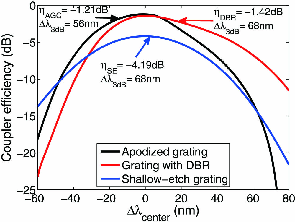
Fig. 1. Calculated coupling efficiencies and 3 dB bandwidth of shallow-etch (SE) GCs with/without DBR and of the AGC.
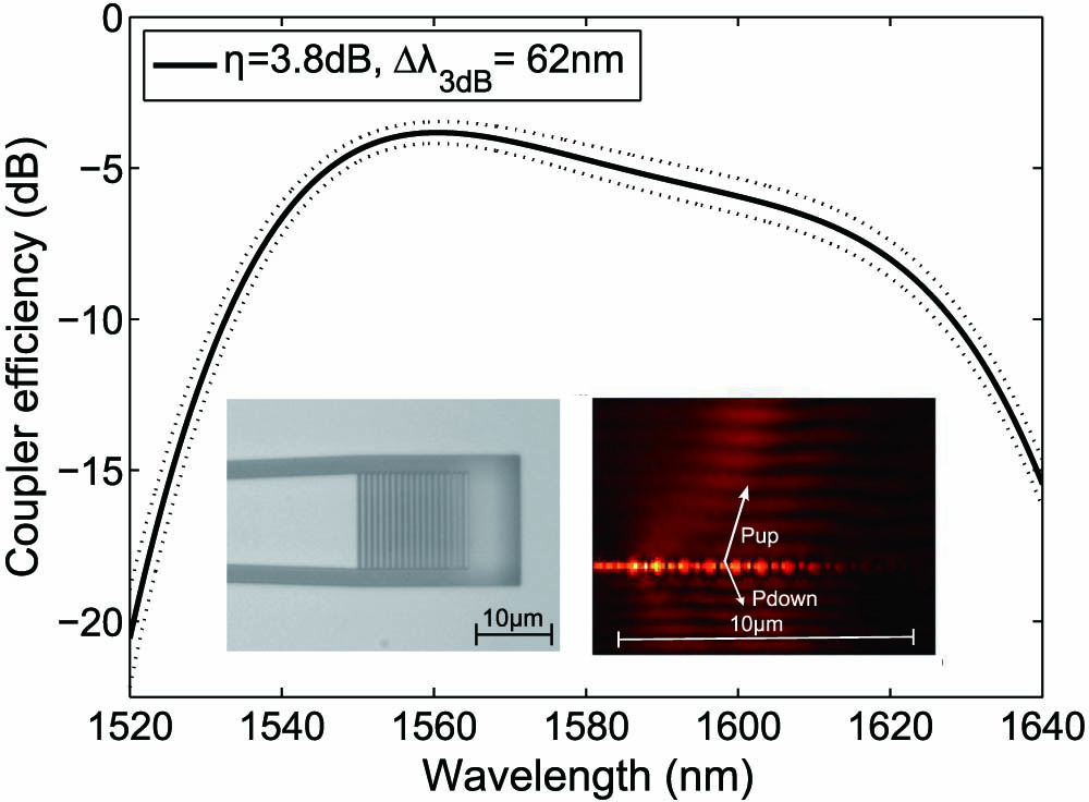
Fig. 2. Measured coupling efficiency of the AGCs with a micrograph and simulation inset.
Fig. 3. Propagation loss measurements for the TE 0
Fig. 4. Power splitting of DCs for different coupler lengths with schematic (inset).
Fig. 5. Bar and cross-port signals of an MZI.
Fig. 6. Spectral characterization of add/drop microring filters: Microring with (a) 5 μm radius and (b) 10 μm radius.
Fig. 7. Q
Fig. 8. (a) Even and odd supermodes of the asymmetric DC with electric field inset. (b) Mode indices of TE 0 TM 0 TE 1
Fig. 9. (a) Measurement setup and micrograph of the PSR. (b) PSR measurements with arbitrary input polarization and polarizer cube set to TE (x y
Fig. 10. Measured tuning efficiency of microheaters placed on top of a 10 μm resonator with microscope picture (inset).
Fig. 11. Resonance shift due to modifications of the effective mode index. Resonance trimming of an uncladded 10 μm MRR blueshifted in 1 nm increments.
Fig. 12. Racetrack-based multiplexer TOE aligned to the 100 GHz DWDM grid with micrograph inset.
Fig. 13. Through- and drop-port spectra of a wavelength-trimmed eight-channel multiplexer with micrograph.
Fig. 14. (a) Spectral disorder of as-fabricated and trimmed OADMs. (b) Static power consumption for the eight-channel assignments of as-fabricated and trimmed OADMs.
Fig. 15. (a) Micrographs of a 4 × 4 I 1 − 4 O 1 − 4 I 1 − O 1 − 3 I 2 − O 2 , 3 , 4 I 3 − O 1 , 2 , 4 I 4 − O 2 − 4
|
Table 1. Nonuniform AGC Parameters
|
Table 2. Linear Loss Comparison of a-SOI/c-SOI Photonic Wires


Set citation alerts for the article
Please enter your email address

© Copyright 2018-2021 | Chinese Laser Press. All Rights Reserved 沪ICP备15018463号-20