Timo Lipka, Lennart Moldenhauer, J?rg Müller, Hoc Khiem Trie, "Photonic integrated circuit components based on amorphous silicon-on-insulator technology," Photonics Res. 4, 0126 (2016)
Copy Citation Text
We present integrated-optic building blocks and functional photonic devices based on amorphous siliconon-insulator technology. Efficient deep-etched fiber-to-chip grating couplers, low-loss single-mode photonic wire waveguides, and compact power splitters are presented. Based on the sub-μmphotonic wires, 2 × 2 Mach–Zehnder interferometers and add/drop microring resonators (MRRs) with low device footprints and high finesse up to 200 were realized and studied. Compact polarization rotators and splitters with ≥10 dB polarization extinction ratio were fabricated for the polarization management on-chip. The tuning and trimming capabilities of the material platform are demonstrated with efficient microheaters and a permanent device trimming method, which enabled the realization of energy-efficient photonic circuits. Wavelength multiplexers in the form of cascaded filter banks and 4 × 4 routers based on MRR switches are presented. Fabrication imperfections were analyzed and permanently corrected by an accurate laser-trimming method, thus enabling eight-channel multiplexers with record low metrics of sub-mW static power consumption and ≤1°C temperature overhead. The high quality of the functional devices, the high tuning efficiency, and the excellent trimming capabilities demonstrate the potential to realize low-cost, densely integrated, and ultralow-power 3D-stacked photonic circuits on top of CMOS microelectronics.
Hydrogenated amorphous silicon (a-Si:H) provides a versatile and low-loss integrated-optic material platform for high index contrast (HIC) photonic circuits. The HIC of , the low absorption loss at the telecommunication bands 1.3–1.55 μm [1,2], and the flexible fabrication capabilities make amorphous silicon-on-insulator (a-SOI) highly attractive for a variety of integrated optic applications. In principle, the material shares the two major advantages of crystalline silicon (c-SOI), which are the high integration density and compatibility to mature complementary metal-oxide semiconductor (CMOS) technology; the almost identical refractive index facilitates the adaptation of existing SOI designs and manufacturing processes.
However, a sharp distinction is evident in the integration approaches: for instance, to realize photonic-electronic-integrated-circuits (PEICs). Whereas c-SOI is first choice for front-end-of-line (FEOL) integration with microelectronics, it does not provide the same flexibility for the integration on top of the microchips at the back-end-of-line (BEOL). Compared with that, it is not practicable to integrate low-loss a-Si:H with FEOL processes because the optical properties start degrading at elevated temperatures () due to dehydrogenation. On the other hand, a-Si:H emphasizes excellent fabrication capabilities to be integrated in multiple layers at the BEOL, including the possibility to integrate FEOL photonics by optical vias. Notwithstanding the limited electrical properties of intrinsic a-Si:H, significant progress has been reported for active photonic devices, e.g., based on pn-doping and/or crystallization [3–7], by deposition on electro-optic substrates [8,9], or all-optically employing the high nonlinear figure of merit [10–12]. Further integration potential includes BEOL-compatible inorganic (AlN, , SiN, , etc.) [13–16], III-V [17–19], and polymer/plasmonic materials [20–22], unfolding the functional capacity of integrated photonics by merging diverse opto-electronic strengths of several materials. Hence, the flexible and low-temperature manufacturing options enable novel concepts to realize hybrid 3D-stacked PEICs.
In this work, we present numerous photonic devices that were fabricated with a-Si:H deposited on top of oxidized Si-wafer substrates and review their functional performances. The components were patterned with electron-beam lithography (EBL) and structured using an advanced silicon deep-etch process [23]. If not stated otherwise, the systems are based on high-confinement photonic wire waveguides (PWs), and the measurement results are reported for the fundamental transverse-electric mode. In Section 2, nonuniform grating couplers (GCs), low-loss PWs, power splitters, and polarization splitters/rotators (PSRs) are studied; functional devices such as microring resonators (MRRs) and Mach–Zehnder-interferometers (MZIs) are presented. Efficient strategies to actively tune photonic devices by integrated microheaters and to permanently adjust components by UV trimming are discussed in Section 3. Optical multiplexers and routers in the form of cascaded filter banks and photonic routers are presented in Section 4. The potential energy savings by the device trimming enabling sub-mW static power consumption for, e.g., eight-channel multiplexers and the anticipated mitigation of the thermal chip budget are discussed.
Sign up for Photonics Research TOC. Get the latest issue of Photonics Research delivered right to you!Sign up now
2. PHOTONIC BUILDING BLOCKS
A. Fiber-to-Chip Grating Couplers
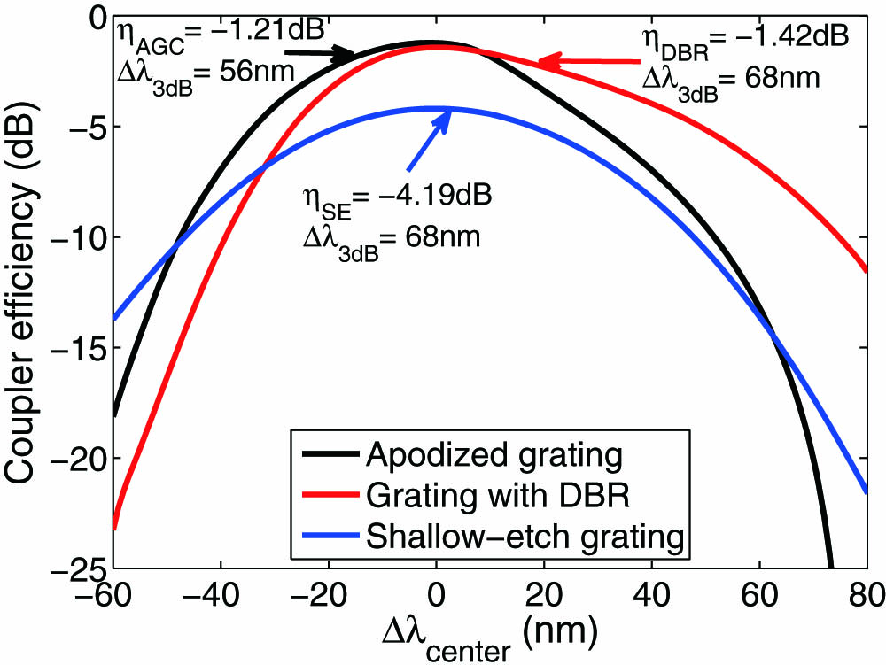
Probably, the most commonly used fiber-chip couplers for HIC photonic circuits are the shallow-etched GCs with a uniform grating period. However, a drawback of this GC type is the coupling efficiency limitation () due to the exponential decay of the guided light along the grating, which is not well matched with single-mode fibers (SMFs) and the fraction of downward diffracted light. In case of a-Si:H, the GC directionality can be increased by bottom reflectors fabricated either by metal layers or by distributed Bragg reflectors (DBRs), which can be deposited prior the bottom silica layer. For instance, a two-stage DBR with layer thicknesses of combined with a standard 65 nm shallow-etch GC with 630 nm half-pitch grating period results in an improved efficiency of but requires considerably more process steps.
From a fabrication viewpoint, it is advantageous to define all photonic structures in one etch step. One solution to achieve this and to overcome the efficiency limitation is the employment of a nonuniform apodized grating coupler (AGC). The apodization minimizes reflections, which are severe for deep-etched uniform GCs, and the optimized duty cycle promotes the radiation of phase fronts that are better matched to the mode profile of optical fibers. The design was adapted to a-SOI wafers with thicknesses ranging from μ with a 200 nm core layer. Parameters of similar devices were taken as starting values [24]; the gap and bar widths were iteratively improved by several optimization loops using the eigenmode expansion method [25]. The nonuniform GC consists of 18 duty cycles; the parameters are summarized in Table 1. The footprint is μμ. The theoretical coupling efficiency to a SMF-28 fiber under a 10°-angle was calculated to be (), comparable with the state of the art [26–29]. The optimized coupling efficiencies of the discussed GC types are provided in Fig. 1.
Figure 1.Calculated coupling efficiencies and 3 dB bandwidth of shallow-etch (SE) GCs with/without DBR and of the AGC.
An optical measurement of the AGC is shown in Fig. 2; the spectra are cleaned from Fabry–Perot reflections that increase approximately from the center wavelength. The coupling efficiency averaged over 12 GCs is about 42% (), the 3 dB bandwidth is with a center wavelength of about 1560 nm for a polymer cladding. The difference to the theoretical limit is most probably attributed to fabrication tolerances caused by lithography and nonuniform etching, particularly in the narrow gaps.
Figure 2.Measured coupling efficiency of the AGCs with a micrograph and simulation inset.
The propagation loss of PWs was determined by virtual cut-back measurements. The linear loss for the fundamental TE mode was determined to be at 1550 nm wavelength, as presented in Fig. 3. The waveguides may include a small loss contribution due to the nonoptimal cladding and by stitching because the meandered waveguides were not patterned within a single EBL writing field (μμ); a homogeneous wafer surface coverage promotes a uniform reactive gas consumption during ICP etching and supports low spectral nonuniformity of the photonic circuit components. Even lower a-Si:H waveguide losses of slightly higher than for SOI have been already demonstrated; benchmark results from the literature are summarized in Table 2. A direct performance comparison of a-Si:H and SOI PWs, bend losses, and couplers with comparable metrics has been recently reported [30].
Figure 3.Propagation loss measurements for the mode. Inset: Mask layout of the meandered waveguides indicating a writing field.
C. Power Splitters and Mach–Zehnder Interferometers
The HIC enables compact power dividers e.g., based on directional couplers (DCs). Experimental results of DCs with a 150 nm coupling gap for coupler length increments of μ are presented in Fig. 4. The graph shows the normalized power splitting between the two output ports at μ. The experimental results are in good agreement with the simulations as verified by the fitting. The offsets at the ordinate originate from the access bends with 20 μm radius. As evident, the 3 dB splitting is achievable with 4 μm long couplers, and any arbitrary split ratio between the bar and cross ports can be realized within μ supporting dense integration. The measurement of a MZI with μ and an arm-length difference of μ is shown in Fig. 5. The FSR of 5.9 nm agrees well with optical simulations, and the 25 dB beat fringe depths of the MZI bar and cross port signals confirm a splitting ratio close to 3 dB.
Figure 4.Power splitting of DCs for different coupler lengths with schematic (inset).
Optical add–drop MRRs belong to the most universally applicable integrated-optic devices and facilitate wavelength-selective filtering functions on a small footprint. We systematically analyzed compact-sized MRRs with 5 and 10 μm radius for different bus-to-ring coupling gaps and evaluated the quality-factor and finesse . Through- and drop-port measurements are provided in Fig. 6. The MRRs exhibit mean FSRs of about 9/18 nm and through-port extinction ratios of for μ, respectively. The average drop losses were determined to be and with drop-port ERs exceeding 25 dB.
Figure 6.Spectral characterization of add/drop microring filters: Microring with (a) 5 μm radius and (b) 10 μm radius.
For a given fabrication process quality and a preliminary choice of the waveguide geometry including the cladding material, the coupling strength is the main parameter that can be used to define the resonator quality. Figure 7 summarizes the loaded -factors and the finesse values that were identified by a Lorentz fit for coupling gaps ranging from 140 to 260 nm. The graph shows that both parameters increase for wider coupling gaps, thus indicating that, within this relatively tight coupling regime, the MRR metrics according to Eq. (1) are governed by the bus-to-ring coupling quality or coupler losses, less limited by the intrinsic quality : Quality factors of were determined for both ring radii and the finesse exceeds and with gaps wider than 240 nm for the 10 and 5 μm MRRs, respectively. The results are comparable with similar dimensioned devices on c-SOI [34,35] and are well-suited for practical applications such as, e.g., biosensing [36] or wavelength-division multiplexing (WDM) [37].
Figure 7.-factor and finesse of 5 and 10 μm radius add/drop filters measured for different coupling gaps.
Highly confined PWs offer significant advantages in terms of small device footprints and scalability compared with lower-index materials; however, they exhibit higher birefringence resulting in different propagation constants of the fundamental TE and TM modes. Hence, on-chip polarization management with rotating and splitting devices is essential in certain types of applications. Efficient polarization splitter-rotators (PSRs) can be, e.g., realized by breaking the horizontal waveguide symmetry due to adjustments of the waveguide shape [38,39] or with asymmetric refractive index cladding materials. In this work, the latter approach has been pursued because the PSR fabrication relies on a single deep-etch process.
The PSR is based on an adiabatic taper for the TM- and TE-mode rotation and an asymmetric DC that performs the polarization mode conversion, as proposed in [40]. The functional principle is illustrated by the dispersion diagram in Fig. 8. The polarization rotation is realized by a flat-angle linear taper that gradually converts to within the hybridized mode region. The PSR is cascaded in three parts: first, the PW widths are widened to 580 nm close to the hybrid region; in the second section, the PW gradually expands with a smooth slope through the hybrid region where is rotated to during transition; finally, the third waveguide section, predominantly guiding and , is tapered for directional coupling. The mode conversion is realized with asymmetric DCs, which transfer to ; however, they leave mostly unaffected due to a large phase-mismatch. The broad waveguide was designed to be 800 nm such that the adapted narrow waveguide of 388 nm in widths provides sufficient guidance in the subsequent curvature. The coupler lengths for a complete power transfer was calculated from the even () and odd () supermodes according to resulting in μ at μ for an air cladding with a fabrication tolerant gap of 150 nm. The overall PSR lengths is approximately 80 μm. The output arms are coupled to MRRs in order to determine the polarization rotation after the PSR due to the wavelength selective filter function.
Figure 8.(a) Even and odd supermodes of the asymmetric DC with electric field inset. (b) Mode indices of , , and versus waveguide widths illustrating the PSR principle.
A picture and the measurement setup are shown in Fig. 9(a). The AGCs were cleaved for the optical characterization using a tunable laser source (TLS) and the chip facet was endfire-coupled with a lensed fiber. The light was collected by a microscope objective at the output, guided through a rotatable polarizer cube via free space, and fiber-collimated to a photo detector (PD). A polarization synthesizer (Agilent N7786B) was utilized to randomly scramble the input light with arbitrary polarization states, and the PSR spectra were measured at both output ports.
Figure 9.(a) Measurement setup and micrograph of the PSR. (b) PSR measurements with arbitrary input polarization and polarizer cube set to TE ( axis) and TM ( axis).
The measurement results are presented in Fig. 9(b). The figure shows the two characteristic MRR spectra for the mode with the polarizer cube oriented to the TE polarization state. The spectra do not show the existence of the mode, and the polarization extinction ratios () at the ports and were measured to be and , respectively. The PSR insertion loss of about 1 dB was determined from reference measurements. The mode conversion efficiency can be further improved by simply cascading PSRs in series at the cost of higher transmission loss and footprint.
3. PHOTONIC DEVICE TUNING AND TRIMMING
Integrated optical devices are susceptible to fabrication inhomogeneities and even sub-nm deviations result in considerable spectral device disorder, which is particularly relevant on a wafer scale. Hence, efficient tuning and trimming strategies for the correction of the photonic circuits are inevitable. Amorphous silicon exhibits excellent material properties for the active tuning of photonic devices by using the strong thermo-optic coefficient , up to 40% higher than for SOI [] [15], and facilitates a permanent correction of photonic components by modifying the refractive index post-fabrication. In the following, the active tuning capabilities with metal microheaters and the passive compensation by laser trimming are discussed.
A. Thermo-optic Tuning by Microheaters
The most prominent method to counteract fabrication imperfections and/or to actively tune photonic circuit components is based on the thermo-optic effect (TOE). The TOE originates from the temperature-dependent refractive material index, which in the following is treated as a real scalar value , suitable for moderate temperatures relevant for PIC tuning. The strong TOE of a-Si:H can be efficiently employed to adjust photonic circuit components with high precision over several nanometers. The temperature-dependent wavelength shift (TDWS) of a MRR is linearly proportional to temperature and is described by with as group index. Photonic chips were gradually heated with by using a temperature-controlled chip mount in order to determine the TDWS and to evaluate the microheater design. Resonance shifts of were measured for 10 μm MRRs with a sputtered cladding.
The integrated microheaters were optimized with the finite element method (COMSOL FEM). The metal heaters were positioned on top of the photonic structures in order to facilitate a good heat transfer to the photonic components with low tuning power and to simplify the routing of the optical and electrical layers. A 1 μm thick cladding was sputtered on top of the bare photonic chips, followed by sputtering titan (Ti) for the heaters and gold (Au) for the bond pads. The microheaters with 2 μm widths and 200 nm thickness were patterned with I-line exposure contact photolithography using alignment markers and reference structures in the a-Si:H core layer and were wet-etched: Au () and Ti ().
The microheater arrays were wire-bonded to a printed circuit board, which was connected to a digital/analog data acquisition card serving as driver. The successive redshift of the drop-port resonance due to different heating powers is shown in Fig. 10. The efficiency on different chips was determined to range between , corresponding to a more universal and ring-size-independent metric of . The deviations result primary from nonuniform wet-etching dependent on the pattern density and can be reduced by lift-off processes. The current heater performance allows tuning a 5 μm MRR over its full FSR of 18 nm with a voltage of about 6.5 V, whereas a 10 μm MRR with 9 nm FSR requires 4.5 V. The microheater efficiency is in line with the best reported values based on SOI devices typically ranging between [41,42]. In principle, due to the higher TOC, higher efficiencies are possible with a-SOI. Further methods that enhance the tuning efficiency with same-dimensioned microheaters include the isolation of the photonic components, e.g., by locally etching the -substrate from the front- or backside [43–45].
Figure 10.Measured tuning efficiency of microheaters placed on top of a 10 μm resonator with microscope picture (inset).
Photonic devices based on HIC materials demand high-precision fabrication, and any perturbation of the guided mode index affects the circuit performance. Although microheaters are ideally suited to actively control photonic circuit components, the correction of manufacturing imperfections dissipates a significant amount of energy and increases the overall thermal load of the photonic chip, which, in turn, demands further run-time compensation. Both effects substantially increase the power budget and may contribute several 10 percents of the overall photonic circuit power [46–48]. Hence, a method that is capable of compensating fabrication tolerances and adjusting the amplitude and phase characteristics of photonic circuit components is advantageous for wafer-scale photonics.
The resonance shift due to a change in guided mode index , which was calculated with an FEM mode solver and numerical calculations, is shown Fig. 11. The results provide that it is possible to trim the MRR spectrum over 10 nm with sub-percentile index modifications. In case of a-Si:H, the material index is trimmable by photolytic processes, so that readily-fabricated PIC devices can be adjusted. The trimming setup, range, velocity, and the tuning accuracy are reported elsewhere [49]. Measurement results of an MRR, which was gradually blueshifted by () with about 20 pm spectral resolution due to UV-laser irradiation with 405 nm wavelength are inset.
Figure 11.Resonance shift due to modifications of the effective mode index. Resonance trimming of an uncladded 10 μm MRR blueshifted in 1 nm increments.
The ability to guide multiple high-data-rate signals within a single waveguide by WDM is a significant property of optical transmission systems. In recent years, high-bandwidth WDM systems have evolved from passive fiber optic communication networks (PONs) down to reconfigurable network-on-chip (NoC) systems [50,51]. In particular, photonic interconnects for high-performance computing and data center communication are promising technologies that could push the technological limits of electronic interconnects that are increasingly affected by RC latency, increased power consumption, and heat generation. Silicon photonics is a potential platform to overcome these bottlenecks because HIC optical interconnects facilitate energy-efficient communication networks with low device footprints fabricated at moderate costs. Integrated optical add/drop multiplexers (OADMs) are essential key devices to perform the selective filtering and routing for these low-power applications [52].
A. Optical Add/Drop Multiplexer
Wavelength multiplexers made of cascaded microrings and racetracks with up to eight channels were realized on a dense 100 GHz grid (). The compact filters were designed to provide a reasonable trade-off between high-data-rate capability, low inter-channel cross talk, and tolerable drop-port loss. The wavelength channels were defined by the ring radii (). The bus-to-ring gaps were outlined with 150 nm for 10 μm radius MRRs. Racetracks with the same curvature were designed with straight coupling sections of 4 μm and 300 nm coupling gaps. For the given parameters, assuming 3 dB propagation and 0.025 dB coupling losses, the simulations reveal drop-port losses of about 1 dB, 15–20 dB inter-channel isolation, and 3 dB bandwidths in the range of 0.18–0.3 nm supporting data rates beyond [37].
Measurement results of a low-footprint four-channel racetrack OADM are presented in Fig. 12; a micrograph is inset. The 3 dB bandwidths are 0.22 nm, the channel cross talk is , and low drop-port losses of about 1.5 dB were determined. The channels are clearly resolved with 30 dB extinction and spaced by 100 GHz. The TOE was employed in order to counterbalance the fabrication imperfections of , which were measured per MRR. In spite of the low spectral nonuniformity from fabrication, a non-negligible steady-state power of is still permanently consumed for the channel alignment using the as-presented top heaters.
Figure 12.Racetrack-based multiplexer TOE aligned to the 100 GHz DWDM grid with micrograph inset.
In this context, we studied the device variability of eight-channel OADMs, as presented in Fig. 13, and evaluated the power requirement for compensation as well as the potential energy savings per device due to the trimming method. The statistical variations of such a-SOI OADMs were determined to range between . Based on our measurements, the channel alignment to the nearest possible ITU specified 100 GHz grid requires about 10–30 mW per eight-channel device. However, this is a simplified scenario because several hundreds to thousands of such devices can be fabricated on a single wafer; hence, the assignment on a wafer-scale is more complex. The process variation of c-SOI MRRs manufactured in CMOS-lines accounts for approximately [53], which, e.g., corresponds to an additional power increase of per channel for top heaters with state-of-the-art performance, if the OADMs are targeted to operate on the same grid. In comparison, on a-SOI and EBL, we determined a similar process variation of about for 50% of the devices and about for [54]. Note that, again, this power is only consumed to equalize the OADM channels relative to each other and the nearest 100 GHz grid and might be significantly higher if an absolute alignment of on-/off-chip lasers with predefined channels is required.
Figure 13.Through- and drop-port spectra of a wavelength-trimmed eight-channel multiplexer with micrograph.
Furthermore, the static tuning of the photonic devices introduces significant local thermal loads, roughly 10°C/cm based on the above metrics, which may affect the photonic link reliability and might require further run-time compensation [55]. Evidently, a passive device trimming, which avoids the overhead tuning power and associated thermal budget and which, in addition, allows assigning athermal filters [16,48] or PICs with hybrid integrated or external sources, is advantageous in terms of energy efficiency. Apart from that, a vertically integrated photonic backplane will be even more challenging from a manufacturing viewpoint, and the PIC nonuniformity will probably be higher than discussed above.
The potential energy savings of the presented OADMs considering only the static power reduction for the nonuniformity compensation are presented in Fig. 14. The channel variability of the as-fabricated multiplexers and the remaining variations after the trimming are shown in Fig. 14(a). The power estimates for the most simplified scenario, which means that the OADMs are configured to the nearest possible 100-GHz grid for top and suspended microheaters ( and ), are presented in Fig. 14(b). The power budget is significantly reduced by more than an order of magnitude down to the sub-mW region per eight-channel device with a thermal load due to alignment, even for top heaters that provide faster switching speed than their under-etched counterparts [42].
Figure 14.(a) Spectral disorder of as-fabricated and trimmed OADMs. (b) Static power consumption for the eight-channel assignments of as-fabricated and trimmed OADMs.
The optical routes of cascaded OADMs are fixed and, hence, link transmitters and receivers in a predefined way. A more versatile concept is based on reconfigurable NoCs, as shown in Fig. 15(a), with MRR switches, which distribute signals among shared optical paths, thereby reducing resources such as lasers and detectors. In the off-resonant state, the signal passes the crossing whereas it can be routed by shifting the MRR on-resonance, e.g., with microheaters. Prototype NoCs with 10 and 20 μm radii MRRs were realized with 260 nm coupling gaps. The crossing with about 1 dB loss is based on a simple design using linear tapers. The devices were characterized in the static case, the results of the 10 μm MRRs are summarized in Fig. 15(b). The rows correspond to the inputs () and the columns to the output ports () that were accessible within this design. The MRRs are undercoupled at 1.55 μm and perform better at 1.6 μm and beyond, where the extinction ratios were determined to be about 10 and 25 dB for the through and drop ports, respectively. The static measurements showcase the potential to realize reconfigurable NoCs in 3D arrangement at BEOL, thus employing a combination of permanent trimming and energy-efficient tuning methods.
Figure 15.(a) Micrographs of a photonic router and a MRR-switch. (b) Static measurements with inputs () and output ports () from top to bottom: Row 1: . Row 2: . Row 3: . Row 4: .
We fabricated and systematically characterized photonic components based on a-SOI material platform. Fiber-to-chip GCs, low-loss PWs, Mach–Zehnder interferometers, and MRRs with key metrics broadly comparable to SOI are reported. Compact power splitters and polarization rotators for on-chip polarization management are presented. The functional quality of the devices is well-suited for practical applications in the areas of biosensing, data-, and telecommunication. Due to the low-deposition temperature, it might be reasonably assumed that devices with comparable quality can be fabricated with low-cost substrate materials such as glasses or even plastics.
The thermo-optic tuning capabilities of a-Si:H material are analyzed, and efficient microheaters with tuning efficiency are demonstrated. Low-footprint wavelength multiplexers and photonic routers are presented. Fabrication imperfections were analyzed and permanently corrected, so that record low metrics of sub-mW consumption per eight-channel multiplexer with temperature introduction due to tuning become feasible. The efficient tuning and accurate trimming capabilities demonstrate the potential to realize low-cost, densely integrated, and ultralow-power 3D-stacked photonic circuits on top of microelectronics.
Acknowledgment
Acknowledgment. This publication was supported by DFG and TUHH in the funding programme Open Access Publishing. Fraunhofer (HHI-Berlin) is acknowledged for EBL.
[38] M. R. Watts, M. Qi, T. Barwicz, L. Socci, P. T. Rakich, E. P. Ippen, H. I. Smith, H. A. Haus. Towards integrated polarization diversity: Design, fabrication and characterization of integrated polarization splitters and rotators. Optical Fiber Communications Conference Technical Digest, PDP11(2005).
[41] M. Watts, W. Zortman, D. Trotter, G. Nielson, D. Luck, R. Young. Adiabatic resonant microrings (arms) with directly integrated thermal microphotonics. Conference on Lasers and Electro-Optics, CPDB10(2009).
Timo Lipka, Lennart Moldenhauer, J?rg Müller, Hoc Khiem Trie, "Photonic integrated circuit components based on amorphous silicon-on-insulator technology," Photonics Res. 4, 0126 (2016)