
Che-Hsuan Huang, Yu-Tang Cheng, Yung-Chi Tsao, Xinke Liu, Hao-Chung Kuo, "Micro-LED backlight module by deep reinforcement learning and micro-macro-hybrid environment control agent," Photonics Res. 10, 269 (2022)
- Photonics Research
- Vol. 10, Issue 2, 269 (2022)
Abstract
1. INTRODUCTION
With the evolution of semiconductor process technology in recent decades, III-V compound semiconductors with excellent direct bandgap features have been extensively employed in various fields such as high-power electronics, lighting, and display technology [1–5]. Light-emitting diodes (LEDs) are the most widely utilized among them in display technology [6,7]. The backlight display technology with LED as the display light source brings superior energy application efficiency and better color quality than traditional display solutions and guides the entire display industry to a thinner design [8–10]. In the last ten years, LED backlight display technology, which was introduced in 2010, has been widely embraced in the global marketplace. There is a more precise blueprint for the future: higher energy application efficiency, higher color saturation, and the micro-LED backlight module with ultrahigh contrast control capability [11–13]. The micro-LED backlight module offers many advantages to foresight displays, but it also brings many novel challenges and innovative opportunities. For example, the quantum-confined Stark effect generated by the thin epitaxial design in the process stage is alleviated using the investigation of the nanosphere photomask etching at NCTU SCLAB [14]. Because of the chip size ratio, the lighting angle design area is limited, posing novel low-light-loss optical design challenges [15]. Quite a few research results have also measured the indirect physical parameters of the overall backlight design [16]. Designing a micro-LED module with both high uniformity and low power consumption remains a critical challenge today. In addition, since quantum dot materials can significantly enhance the color quality of displays, quantum dot color conversion technology is also an extremely important and widely discussed technology in forward-looking display technology [17,18].
Many mature approaches and physical concepts of optical design have been established and utilized in various research efforts during the last half-century. In the field of LED, there is a great deal of research and analysis on physical models of different scales [19–27]. However, since the specific manifestations of macro-scale and micro-scale exhibit particle and wave, it is often impossible to design both macro-scale and micro-scale at the same time when performing optical design. This phenomenon has become a challenging issue for micro-LED modules that pursue ultrathin design since the micro-scale of the crystal grain structure and the macro-scale of the backlight module are both present in the micro-LED module [28,29]. This paper constructs a set of the optical programming process and introduces an environmental control agent technology to control the macro- and micro-scale. Furthermore, due to the traditional optimization calculation methods such as differential evolution and genetic algorithms, all are rule-based algorithms, which are characterized by interpretability and the use of fewer hyperparameters. Although this method is convenient for developers to use, it is more difficult to apply to topics with greater variability. On the contrary, a data-driven algorithm driven by a large amount of data has many hyperparameters to solve various changing problems. In order to achieve a highly adaptable solution, and to avoid overly sensitive search processes that lead to the inability to find the global maximum or minimum value, this study provides artificial intelligence deep reinforcement learning technology and employs Google DeepMind’s double DQN (DDQN) architecture as the core network to create artificial intelligence optical design agents for optimum optical design [30–33]. Deep reinforcement learning (DRL) and environment control agent technology are fully implemented in this research [34–40]. In addition, based on the inference results of the artificial intelligence model, it successfully produces ultrathin, high-efficiency, high-uniformity micro-LED modules.
2. EXPERIMENT AND ALGORITHM DESIGN
A. Introduction of the Micro-LED Module and Optical Events
In the application of foresight displays, the micro-LED backlight module is the current mainstream developing technology. A complete micro-LED backlight module is shown in Fig. 1. The main structure contains the substrate, the receiver plane; the LED array, which has a wavelength spectrum with Gaussian distribution in which the peak of the spectrum is at 445 nm and the width of spectrum is 18 nm; and the structure design on the LED. In this paper, a distributed Bragg reflector (DBR) structure is selected as the structure to control the light-emitting angle of the LED as shown in Fig. 1(b), covering each LED under the LED array. In this module structure, there are four main types of optical events when the light is emitted from the LED to the receiver plane.
Sign up for Photonics Research TOC. Get the latest issue of Photonics Research delivered right to you!Sign up now
Due to the four abovementioned optical events, the light generates many reflection events between the receiver plane, the DBR, and the substrate. If a reflection is not incident on a perfectly reflective surface, it causes energy loss in the optical system. To reduce the loss, in the module design, a high-reflectivity coating is used for coating on the substrate surface as shown in Fig. 1(c), and the diffuser plate with an etched pattern is used as the receiver plane as shown in Fig. 1(d). To reduce the energy loss, the substrate is coated by a thick
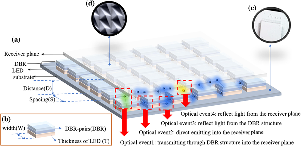
Figure 1.(a) Schematic diagram of micro-LED backlight module; (b) schematic diagram of LED with DBR structure; (c) highly-reflective surface substrate; (d) etching structure of the receiver.
After completing the frame design of the module, the important variables that should be taken into consideration in designing the micro-LED backlight module are indicated in Figs. 1(a) and 1(b).
This study will develop an optimization approach for the architecture’s four-variable design.
B. Overall Design Workflow
As shown in Fig. 2, we provide a comprehensive set of design methodologies for achieving perfect simulation and optimization results. This design process is divided into two major modules. One is the optimization engine for deep reinforcement learning as shown in Fig. 2(a). The task of the module is to optimize the design of artificial intelligence design agents in a controlled environment. The other core module is simulation verification, such as Fig. 2(b). This verification aims to ensure that the environment of the design model is consistent with the actual field. Thus, the gap is small enough to have a sufficient degree of reliability between the analog design and the implementation.
![]()
Figure 2.Workflow for optimizing micro-LED backlight module: (a) the process of deep reinforcement learning and (b) the process of the virtual-realistic experiment.
Figure 2(a) shows that two core modules make up the optimization engine, namely, the designing agent and the environment. After the designing agent issues a specified action to the environment for execution each time, the environment reports the environment state and reward to the designing agent. The algorithm network in the designing agent learns deep neural network (DNN) and guides the policy function to give the following action. After multiple iterations when the reward is saturated, optical design optimization can be obtained. The neural network model used in this paper is the double deep Q-learning neural (DDQN) network model published by Google in 2015, with
Another part that has a significant impact on the design results is the environment in the reinforcement learning architecture. Since the micro-LED backlight module has both a nano-level structure and a millimeter-level module structure, macro-scale and micro-scale operations must be taken into account. Wave optics, in general, dominate the calculation of the micro-scale; this paper uses Synopsys’ R-soft software for calculations. On the other hand, macro-scale calculation generally uses geometric optics for optical calculation; this paper adopts Synopsys’ LightTools software for calculations. Although there are sophisticated computer-aided engineering (CAE) tools that can handle micro- and macro-scale problems separately, the micro-LED backlight module must deal with two extreme dimensions at once, and thus we add the notion of environment control agent and container into the environment as shown in the environment in Fig. 2(a). We set the environment and database required for the operation of LightTools and R-soft separately in the environment design, and then we utilize the environment agent program to perform collaborative scheduling of the two container tasks. Through the environment control agent and independent container settings, we can effectively solve extreme-scale computing problems.
After completing the environment architecture based on the environment control agent and containers, as shown in Fig. 2(b), to accomplish high-reliability simulation, we undertake two sets of extreme environment individual parameter verifications between the virtual environment and the actual scene, which we term a virtual-realistic experiment. In the virtual-realistic experiment, we compare the completed micro-LED array sample image with the LightTools simulation image and quantify the difference through validation to obtain the best combination of realistic parameters. Similarly, we also use the completed micro-LED with DBR structure to compare with R-soft’s simulation result image and quantify the difference through validation to obtain the best realistic parameter combination.
This paper will use the optimized architecture of Fig. 2(a) and the immersive environment setting of Fig. 2(b) to design a highly reliable micro-LED backlight module.
C. Establishing an Environment Control Agent
The workflow of establishing environment is as shown in Fig. 3(a). To begin, we implement the first batch of micro-LED backlight module prototypes, capture images using a CMOS sensor, and use single chip and chip array images as a baseline for optimizing simulation parameters. On the other hand, the optical simulation models of the DBR and micro-LED backlight module were built using R-soft and LightTools, respectively. There are six groups of experimental combinations:
In the simulation, the backlight module’s bottom reflectivity and receiver reflectivity are the essential systematic variables. To establish close-to-accurate environmental parameters, the optical reflection characteristics of actual samples generally have scattering characteristics. The scattering mode of reflected light is roughly divided into Gaussian type (the angle between the main direction of the reflected light and the normal is consistent with the incident angle) and Lambertian type (the reflected light at any angle of incidence is scattered along the normal direction) as shown in Fig. 3(b). We perform simulation calculations on the bottom reflectivity and receiver reflectivity for two scattering modes and five variables (Gaussian type 0°, Gaussian type 5°, Gaussian type 10°, Gaussian type 15°, and Lambertian type). The schematic diagram of the scattering model is as shown in Fig. 3(b). The variable intervals of bottom reflectivity and receiver reflectivity are 93%–99% and 20%–40%, respectively; after completing the simulation calculation, the result matrix output of the simulation calculation and the image collected by CMOS are calculated for validation as shown in Fig. 2(b). The calculation is calculated by mean-square error as Eq. (1):
![]()
Figure 3.(a) Workflow of environment control agent and schematic diagram of the virtual-realistic experiment; (b) principle of kernel1: Gaussian and Lambertian reflection; (c) principle of kernel2: BSDF properties.
After completing the MSE calculation of the virtual-realistic experiment, we take the parameter combination when the MSE is minimum as the basic parameters of the environment model. The equation is expressed as Eq. (2):
After completing the value of the environment parameters, we set up the environments of the micro-scale and macro-scale in PC2 and PC3 computers, respectively. PC2 constructs a computing core based on the micro-scale, and its environment is called container2. The computing kernel in container2 is thin-film optics, and the main database is the thin-film database, which contains various film material characteristic values such as refractive index
D. Definition of Action Function, State Function, and Reward Function
It can be seen from Fig. 2(a) that in reinforcement learning, there are three functions, action, state, and reward, that should be defined between the environment and the designing agent. Referring to the design parameters in the schematic diagrams of Figs. 1(a) and 1(b), we define the action function as Table 1. For the five kinds of variations to adjust up and down, we defined the action functions of a1–a10. In addition, we also define the state function of S1 to S5 for the five variation states as shown in Table 2. Finally, referring to the definition of uniformity of the backlight module, we have set three different reward functions as Eqs. (3)–(5):
Among them, Eq. (3) adopts the floating reward computer system, while Eqs. (4) and (5) adopt the computer system of fixed uniformity comparison method. First, we need to define the environment’s boundary value before executing the reinforcement learning calculation. The environment parameters are as Table 3.
Definition List of Action
| Action No. | Action Definition | Variation Symbol |
|---|---|---|
| Add distance | ||
| Reduce distance | ||
| Add width | ||
| Reduce width | ||
| Add spacing | ||
| Reduce spacing | ||
| Add thickness | ||
| Reduce thickness | ||
| Add DBR pairs | DBR | |
| Reduce DBR pairs | DBR |
Definition List of State
| State No. | State Definition | Variation symbol |
|---|---|---|
| Value of distance | ||
| Value of spacing | ||
| Value of DBR pairs | ||
| Value of thickness | ||
| Value of width | DBR |
Definition List for Range of Parameters
| No. | Parameters | Variation | Range |
|---|---|---|---|
| 1 | Distance from receiver to LED | 100–180 μm | |
| 2 | LED width | 10–100 μm | |
| 3 | LED spacing | 300–700 μm | |
| 4 | Thickness of LED | 5–55 μm | |
| 5 | DBR-BSDF pairs | DBR | 4.5–9.5 pairs |
E. Double Deep Q-learning Neural Network
As shown in Fig. 2(a), the double DQN (DDQN) network is used as the optimized algorithm in this paper. The detailed calculation process is shown in Fig. 4. The action (
![]()
Figure 4.Workflow of DDQN network.
After multiple iterations, an optimal result can be obtained when the loss function value converges.
3. RESULT
A. Virtual-Realistic Experiment
The parameter setting of the environment construction is often an essential element that determines the accuracy of the final model. This paper starts the virtual-realistic experiment when the environment is built. According to the actual sample production, we use GaN as the epitaxial structure of the wafer and use AlN/GaN as a DBR structural material, and its related fixed parameters are shown in Table 4. The experimental results are shown in Fig. 5. According to Fig. 5(a), we show the actual shooting results of a single chip with no DBR structure, 2.5 pairs DBR, and 5.5 pairs DBR, and the results of MSE calculation on the image after changing the bottom reflectivity. As a result, the curves of the Gaussian type are all lower than the Lambertian type, and the minimum value can be found when reflectivity is 97%. From the experimental results, we can choose the parameters with the lowest MSE: Gaussian
Results of Virtual-Realistic Experiment
| No. | Parameters | Value |
|---|---|---|
| 1 | Bulk of GaN-based light-emitting diodes | Refraction |
| 2 | High-reflectivity white bottom surface of module | Gaussian type 5° with 97% |
| 3 | Receiver reflectivity | Lambertian with 35% |
| 4 | Index of DBR material (AIN/GaN) | |
| 5 | Thickness of DBR material (AIN/GaN) |
![]()
Figure 5.Virtual-realistic experiment: (a) single light pattern analysis; (b) module pattern analysis.
In addition, according to Fig. 5(b), we show the experimental results of the array type. The experimental results of the array type are mainly used to calculate the best receiver reflectivity. In the actual sample, the receiver is a PMMA structure with a surface etching pattern. The main optical mechanisms of this structure are mostly reflection, scattering, and refraction. In this experimental result, the Lambertian type has a lower MSE calculation result, and the Lambertian type has the lowest MSE value when the reflectivity is 35%, so the Lambertian type, receiver
B. Result of Reinforcement Learning
After constructing the environment, we use DDQN network for reinforcement learning and set three different reward functions and parameter optimization boundaries in reinforcement learning, such as Tables 3 and 4. The design of reward function1 is defined as “strict decreasing,” which means it is required that each loss must be lower than the previous one. Besides, reward function2 and reward function3 are defined as the reward function compared with a fixed reference value. Since reward functions2 and 3 do not need to follow strict incremental rules, they can avoid overfitting and have a more stable convergence result.
The experimental results are shown in Figs. 6(a), 6(b), and 6(c), respectively, representing uniformity for every iteration with reward functions 1, 2, and 3. The iteration results using reward function1 are volatile initially, and results with a uniformity of 0 often appear. Although it does not reach the more stable operation optimization until after 250 iterations, the value can still discover a significant attenuation instability result in the stable area. The best result appears in the 289th iteration. The result is shown in Fig. 6(d). According to the value of the average
![]()
Figure 6.Result of reinforcement learning: (a) uniformity for every iteration with reward function1; (b) uniformity for every iteration with reward function2; (c) uniformity for every iteration with reward function3; (d) the best result by reward function1; (e) the best result by reward function2; (f) the best result by reward function3.
Figure 6(d) shows that the state of the best solution when calculating reward function1 is
C. Result of Real Sample
After completing the optimized model design above, we made a prototype demonstration according to the
![]()
Figure 7.Demonstration of the micro-LED backlight module.
4. DISCUSSION
According to the above experimental results, the designing agent designed by the method proposed in this paper can effectively optimize the optical design, but more physical characteristics still need to be summarized. We will focus on the following points and discuss them.
A. Inference of DBR Structure
First, we set the state
![]()
Figure 8.Influence of DBR structure: (a) light pattern with state
B. Energy Loss Mechanism of the Micro-LED Backlight Module
We can observe from the above results that DBR can optimize the light energy of the dark band by reflecting the light of the chip. In the process, each reflection is often accompanied by energy loss as shown in Fig. 9. The light loss generated by the light reflected by the DBR structure to the backplane is the main energy loss mechanism of the micro-LED backlight module, and the other is the light loss caused by the light reflected by the receiver to the backplane as shown in Fig. 1. The structure of the micro-LED backlight module uses a high-thickness and highly-reflective filler surface reflective paint structure from the beginning of the architecture due to the consideration of optical event3 and optical event4. This structure is concluded to have a reflectivity of up to 97% in the results of the virtual-realistic experiment, allowing the optical loss of the entire system to reduce to within 10%.
![]()
Figure 9.Schematic of resonant loss for the micro-LED backlight module.
C. Designing Rule of the Micro-LED Backlight Module
Table 5 provides the optimization results under different reward function designs.
Best Uniformity for Different Reward Functions
| Best State | Reward Formula | Parameters | Number of Iterations | Best |
|---|---|---|---|---|
| 289 | 83.97% | |||
| 183 | 86.51% | |||
| 249 | 90.32% |
The
D. Work Efficiency of Reinforcement Learning
In this study, a high-efficiency designing agent is established through reinforcement learning and environment control agent. To ensure that the solution obtained by the designing agent within the parameter limit interval is the best, step is added to the lower limit interval defined in the
Work Efficiency of Designing Agent
| Number of | Time | Optimal | |
|---|---|---|---|
| Entire loop | 106,920 | 297 | Uniformity: 89.61% |
| Designing agent | 16,000 | 53.3 | Uniformity: 90.32% |
According to Table 6, although the entire loop seems to describe the complete solution plane, since the steps of each parameter are fixed values, the solution plane depicted by the entire loop is a plane depiction of a discrete solution. On the other hand, it adopts the designing agent of reinforcement learning that has the characteristics of a deep learning solution, which is to narrow the search range to find the best solution. Therefore, it can provide more efficient and superior optimization solutions.
5. CONCLUSION
Traditional optical design methods generally emphasize the accuracy of model parameters. There are many studies on measuring detailed parameters; however, considering the influence of extreme scales at the same time can be challenging. The environment control agent technology introduced in this research efficiently integrated micro-scale and macro-scale models into a single set of optimization models, eliminating all calculation barriers imposed by different calculation scales. A high-efficiency model optimization design method for micro-LED backlight modules is also provided by the reinforcement learning model.
In comparison to the entire loop mode, a higher resolution optimal position on the solution plane can be determined; hence, the designing agent’s optimization result is somewhat better than that of the entire loop. Besides, compared with the multi-parameter discrete loop solution, the designing agent can find a more accurate solution, and it only needs 17.9% of the entire loop time to find a solution. This research successfully developed a micro-LED backlight module with a DBR structure as the backlight uniformity optimization element using a novel multi-environment control approach and reinforcement learning framework. Its uniformity has improved by 32% when compared to a micro-LED backlight module without a DBR structure.
Acknowledgment
Acknowledgment. The authors thank LEDA-technology Co., Ltd. for technical support in advising of programing and deep learning.
References
[1] I. C. Kizilyalli, A. P. Edwards, H. Nie, D. Disney, D. Bour. High voltage vertical GaN p-n diodes with avalanche capability. IEEE Trans. Electron Devices, 60, 3067-3070(2013).
[2] S. Han, S. Yang, K. Sheng. High-voltage and high-
[3] J. Wang, L. Cao, J. Xie, E. Beam, R. McCarthy, C. Youtsey, P. Fay. High voltage, high current GaN-on-GaN p-n diodes with partially compensated edge termination. Appl. Phys. Lett., 113, 023502(2018).
[4] S. Pimputkar, J. Speck, S. DenBaars, S. Nakamura. Prospects for LED lighting. Nat. Photonics, 3, 180-182(2009).
[5] C.-H. Huang, K.-J. Chen, M.-T. Tsai, M.-H. Shih, C.-W. Sun, W.-I. Lee, C.-C. Lin, H.-C. Kuo. High-efficiency and low assembly-dependent chip-scale package for white light-emitting diodes. J. Photon. Energy, 5, 057606(2015).
[6] T. Wu, C.-W. Sher, Y. Lin, C.-F. Lee, S. Liang, Y. Lu, S.-W. H. Chen, W. Guo, H.-C. Kuo, Z. Chen. Mini-LED and micro-LED: promising candidates for the next generation display technology. Appl. Sci., 8, 1557(2018).
[7] R. S. West, H. Konijn, W. Sillevis-Smitt, S. Kuppens, N. Pfeffer, Y. Martynov, Y. Takaaki, S. Eberle, G. Harbers, T. W. Tan, C. E. Chan. 43.4: high brightness direct LED backlight for LCD-TV. SID Symp. Dig. Tech. Pap., 34, 1262-1265(2003).
[8] Z. Luo, Y. Chen, S.-T. Wu. Wide color gamut LCD with a quantum dot backlight. Opt. Express, 21, 26269-26284(2013).
[9] C. H. Huang, C. Y. Kang, S. H. Chang, C. H. Lin, C. Y. Lin, T. Wu, C. W. Sher, C.-C. Lin, P.-T. Lee, H.-C. Kuo. Ultra-high light extraction efficiency and ultra-thin mini-LED solution by freeform surface chip scale package array. Crystals, 9, 202(2019).
[10] S. Kikuchi, Y. Shibata, T. Ishinabe, H. Fujikake. Thin mini-LED backlight using reflective mirror dots with high luminance uniformity for mobile LCDs. Opt. Express, 29, 26724-26735(2021).
[11] F.-C. Lin, Y.-P. Huang, L.-Y. Liao, C.-Y. Liao, H.-P. D. Shieh, T.-M. Wang, S.-C. Yeh. Dynamic backlight gamma on high dynamic range LCD TVs. J. Display Technol., 4, 139-146(2008).
[12] G. Tan, Y. Huang, M.-C. Li, S.-L. Lee, S.-T. Wu. High dynamic range liquid crystal displays with a mini-LED backlight. Opt. Express, 26, 16572-16584(2018).
[13] H. Chen, R. Zhu, M.-C. Li, S.-L. Lee, S.-T. Wu. Pixel-by-pixel local dimming for high-dynamic-range liquid crystal displays. Opt. Express, 25, 1973-1984(2017).
[14] S.-W. H. Chen, Y.-M. Huang, K. J. Singh, Y.-C. Hsu, F.-J. Liou, J. Song, J. Choi, P.-T. Lee, C.-C. Lin, Z. Chen, J. Han, T. Wu, H.-C. Kuo. Full-color micro-LED display with high color stability using semipolar (20-21) InGaN LEDs and quantum-dot photoresist. Photon. Res., 8, 630-636(2020).
[15] E.-L. Hsiang, Z. He, Y. Hung, F. Gou, Y.-F. Lan, S.-T. Wu. Optimal chip size for reducing the power consumption of micro-LED displays. Proc. SPIE, 11708, 117080M(2021).
[16] C.-H. Huang, S. H. Chang, B.-Y. Liaw, C.-Y. Chou, C.-C. Lin, H.-C. Kuo, L.-J. Song, F. Li, X. Liu. Research on a novel GaN-based converted mini-LED backlight module via a spectrum-decouple system. IEEE Access, 8, 138823-138833(2020).
[17] E. Chen, J. Guo, Z. Jiang, Q. Shen, Y. Ye, S. Xu, J. Sun, Q. Yan, T. Guo. Edge/direct-lit hybrid mini-LED backlight with U-grooved light guiding plates for local dimming. Opt. Express, 29, 12179-12194(2021).
[18] E. Chen, H. Xie, J. Huang, H. Miu, G. Shao, Y. Li, T. Guo, S. Xu, Y. Ye. Flexible/curved backlight module with quantum-dots microstructure array for liquid crystal displays. Opt. Express, 26, 3466-3482(2018).
[19] H.-R. Moon, M.-H. Shin, J.-Y. Lee, K.-J. Jang, Y.-O. Chung, Y.-J. Kim. Design of integrated light guide plate with functional structure of enhanced diffusion length for ultra-slim LED backlight unit. J. Display Technol., 11, 768-775(2015).
[20] S. Wang, K. Wang, F. Chen, S. Liu. Design of primary optics for LED chip array in road lighting application. Opt. Express, 19, A716-A724(2011).
[21] W.-S. Oh, D. Cho, K.-M. Cho, G.-W. Moon, B. Yang, T. Jang. A novel two-dimensional adaptive dimming technique of X-Y channel drivers for LED backlight system in LCD TVs. J. Disp. Technol., 5, 20-26(2009).
[22] J. H. Lee, S. G. Han, M. J. Jin. Minimum achievable height of a single-module LED low-beam projection headlamp. Appl. Opt., 60, E8-E16(2021).
[23] R. J. Lin, M.-S. Tsai, C.-C. Sun. Novel optical lens design with a light scattering freeform inner surface for LED down light illumination. Opt. Express, 23, 16715-16722(2015).
[24] B.-Y. Joo, J.-H. Ko. Analysis of color uniformity of white LED lens packages for direct-lit LCD backlight applications. J. Opt. Soc. Korea, 17, 506-512(2013).
[25] S.-L. Hsiao, N.-C. Hu, H. Cornelissen. Phosphor-converted LED modeling using near-field chromatic luminance data. Opt. Express, 21, A250-A261(2013).
[26] S.-S. Schad, B. Neubert, C. Eichler, M. Scherer, F. Habel, M. Seyboth, F. Scholz, D. Hofstetter, P. Unger, W. Schmid, C. Karnutsch, K. Streubel. Absorption and light scattering in InGaN-on-sapphire- and AlGaInP-based light-emitting diodes. J. Lightwave Technol., 22, 2323-2332(2004).
[27] N. Pendam, C. P. Vardhani. Design and simulation of asymmetrical Y-branch optical power splitter on SOI platform and study the propagation loss with branching angle, index difference, and slab height. 13th International Conference on Fiber Optics and Photonics, W3A.44(2016).
[28] A. D. Griffiths, J. Herrnsdorf, R. K. Henderson, M. J. Strain, M. D. Dawson. High-sensitivity inter-satellite optical communications using chip-scale LED and single-photon detector hardware. Opt. Express, 29, 10749-10768(2021).
[29] X. Li, L. Wu, Z. Liu, B. Hussain, W. C. Chong, K. M. Lau, C. P. Yue. Design and characterization of active matrix LED microdisplays with embedded visible light communication transmitter. J. Lightwave Technol., 34, 3449-3457(2016).
[30] P. S. Rajendran, A. Geetha. Optimization of hospital bed occupancy in hospitals using double deep Q network (DDQN). 3rd International Conference on Intelligent Communication Technologies and Virtual Mobile Networks (ICICV), 1029-1033(2021).
[31] X. Huang, W. Luo, J. Liu. Attitude control of fixed-wing UAV based on DDQN. Chinese Automation Congress (CAC), 4722-4726(2019).
[32] M. G. P. de Lacerda, F. B. de Lima Neto, H. de Andrade Amorim Neto, H. Kuchen, T. B. Ludermir. On the learning properties of dueling DDQN in parameter control for evolutionary and swarm-based algorithms. IEEE Latin American Conference on Computational Intelligence (LA-CCI), 1-6(2019).
[33] B. Wang, Y. Li, W. Ming, S. Wang. Deep reinforcement learning method for demand response management of interruptible load. IEEE Trans. Smart Grid, 11, 3146-3155(2020).
[34] B. C. Sanders, P. Palittapongarnpim, S. S. Vedaie. Reinforcement learning for adaptive optical quantum-enhanced metrology. Imaging and Applied Optics 2018, STu5H.4(2018).
[35] X. Hu, A. Schülzgen. Design of negative curvature hollow core fiber based on reinforcement learning. J. Lightwave Technol., 38, 1959-1965(2020).
[36] S. P. K. Karri, D. Chakraborthi, J. Chatterjee. Learning layer-specific edges for segmenting retinal layers with large deformations. Biomed. Opt. Express, 7, 2888-2901(2016).
[37] R. Zhu, S. Li, P. Wang, L. Li, A. Samuel, Y. Zhao. Deep reinforced energy efficient traffic grooming in fog-cloud elastic optical networks. Optical Fiber Communication Conference (OFC), M1A.4(2020).
[38] Q. Chen, M. Zhu, T. Shen, J. Gu, C. Yan, P. Gu. Deep-reinforce-learning-assisted network orchestration for VNF-SC provisioning in inter-DC elastic optical networks. Asia Communications and Photonics Conference/International Conference on Information Photonics and Optical Communications (ACP/IPOC), M4A.185(2020).
[39] L. Moro, E. Prati. Optical manipulation of qubits by deep reinforcement learning. OSA Quantum 2.0 Conference, QM6A.4(2020).
[40] X. Wang, Y. Huang, J. Liu, S. Yu. A subcarrier-slot autonomous partition scheme based on deep-reinforcement-learning in elastic optical networks. Asia Communications and Photonics Conference (ACPC), M4A.211(2019).


Set citation alerts for the article
Please enter your email address

© Copyright 2018-2021 | Chinese Laser Press. All Rights Reserved 沪ICP备15018463号-20