[1] D. B. Holt, D. C. Joy. SEM Microcharacterization of Semiconductors(1989).
[2] J. Goldstein, D. Newbury, D. Joy, C. Lyman, P. Echlin, E. Lifshin, L. Sawyer, J. Michael. Scanning Electron Microscopy and X-ray Microanalysis(2007).
[3] L. Reimer. Scanning Electron Microscopy: Physics of Image Formation and Microanalysis(1998).
[4] W. Zhou, Z. L. Wang. Scanning Microscopy for Nanotechnology: Techniques and Applications(2007).
[5] A. J. Schwartz, M. Kumar, B. L. Adams, D. P. Field. Electron Backscatter Diffraction in Materials Science(2009).
[15] B. G. Yacobi, D. B. Holt. Cathodoluminescence Microscopy of Inorganic Solids(1990).
[22] E. A. Holm, A. Winkelmann, S. Farjami, G. Nolze, P. Manohar, M. Himmerlich, G. Rohrer, V. Lebedev, A. D. Rollett, A. Reichmann, D. Srolovitz, H. Weiland. Point-group sensitive orientation mapping using EBSD. Proceedings of the 6th International Conference on Recrystallization and Grain Growth, 281-286(2016).
[29] H. G. J. Moseley. The high-frequency spectra of the elements. Philos. Mag., 27, 703-713(1914).
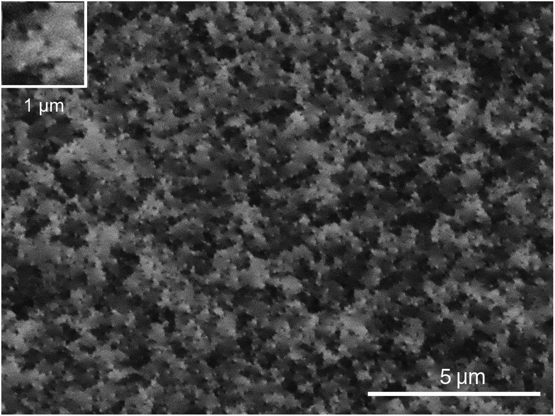
[42] P. M. Coulon, B. Damilano, B. Alloing, P. Chausse, S. Walde, J. Enslin, R. Armstrong, S. Vézian, S. Hagedorn, T. Wernicke, J. Massies, J. Zúñiga‐Pérez, M. Weyers, M. Kneissl, P. A. Shields. Displacement Talbot lithography for nano-engineering of III-nitride materials. Microsyst. Nanoeng.,(2019).