C. Trager-Cowan1,*, A. Alasmari1, W. Avis1, J. Bruckbauer1..., P. R. Edwards1, B. Hourahine1, S. Kraeusel1, G. Kusch1, R. Johnston1, G. Naresh-Kumar1, R. W. Martin1, M. Nouf-Allehiani1, E. Pascal1, L. Spasevski1, D. Thomson1, S. Vespucci1, P. J. Parbrook2, M. D. Smith2, J. Enslin3, F. Mehnke3, M. Kneissl3,4, C. Kuhn3, T. Wernicke3, S. Hagedorn4, A. Knauer4, V. Kueller4, S. Walde4, M. Weyers4, P.-M. Coulon5, P. A. Shields5, Y. Zhang6, L. Jiu6, Y. Gong6, R. M. Smith6, T. Wang6 and A. Winkelmann1,7|Show fewer author(s)
Abstract
In this paper we describe the scanning electron microscopy techniques of electron backscatter diffraction, electron channeling contrast imaging, wavelength dispersive X-ray spectroscopy, and cathodoluminescence hyperspectral imaging. We present our recent results on the use of these non-destructive techniques to obtain information on the topography, crystal misorientation, defect distributions, composition, doping, and light emission from a range of UV-emitting nitride semiconductor structures. We aim to illustrate the developing capability of each of these techniques for understanding the properties of UV-emitting nitride semiconductors, and the benefits were appropriate, in combining the techniques.1. INTRODUCTION
The scanning electron microscope (SEM) is a very powerful tool for investigating and imaging a wide range of material properties spanning topography, structure, composition, and light emission [1–4]. SEMs are extensively used for imaging topography by monitoring the intensity of secondary electrons as a focused electron beam, with an energy in the range of 100 eV to 30 keV rastered over the surface of a sample. Less well known are the techniques of electron backscatter diffraction (EBSD) [5–8] and electron channeling contrast imaging (ECCI) [6,8–14], which exploit diffraction to provide information on crystal structure, crystal misorientation, grain boundaries, strain, and structural defects, such as dislocations and stacking faults. Using the techniques of energy dispersive spectroscopy or wavelength dispersive spectroscopy (WDX), emitted X-rays may be used to provide compositional information [1,2]. The light emission cathodoluminescence (CL) [15–17] and the current (electron beam-induced current) [1,17] generated when a high-energy electron beam is incident on a sample, provide valuable information on a sample’s luminescence and electrical properties, respectively. While each of these techniques individually provides valuable information, when one or more of these techniques are combined, they can provide invaluable complementary information. For example, as we illustrate in this paper, it is possible to acquire an ECCI micrograph and a CL image for the same part of the sample to determine the influence of structural defects on a material’s light emission properties.
In this paper we describe the SEM techniques of EBSD, ECCI, WDX, and CL hyperspectral imaging and illustrate the capability (and also the shortcomings) of each technique. To this end we present our recent results on the use of these non-destructive techniques to obtain information on the topography, crystal misorientation, defect distributions, composition, doping, and light emission from a range of UV-emitting nitride semiconductor structures. We also give examples where combining the techniques provided useful complementary information.
In comparison to their visible cousins, UV LEDs based on nitride semiconductor thin films exhibit poor electro-optical properties with external quantum efficiencies typically no more than 10% for wavelengths less than 350 nm [18]. Their ultimate performance is presently limited by the structural quality of AlN and AlGaN thin films, which limits the achievable internal quantum efficiency, and by low doping efficiencies, low carrier injection efficiencies, and poor light extraction [19]. Key to improving the performance of UV LEDs, and the main motivation for the research described in this paper, is (1) the understanding and control of extended defects, such as grain boundaries, threading dislocations, partial dislocations, and stacking faults and their influence on light emission; (2) the control of doping; and (3) control of the alloy composition of AlGaN.
Sign up for Photonics Research TOC. Get the latest issue of Photonics Research delivered right to you!Sign up now
To carry out our measurements we use a range of SEMs equipped with both commercial and bespoke detection systems. In the work reported here we have used an FEI Sirion 200 Schottky field emission gun SEM (Sirion SEM) equipped with an in-house developed ECCI system. We have also used an FEI Quanta 250 Schottky field emission gun environmental/variable pressure SEM (Quanta SEM) equipped with an Oxford Instruments Nordlys EBSD detector and forescatter diodes for EBSD and ECCI measurements, respectively, and an in-house developed CL hyperspectral imaging system. The CL system utilizes a Schwarzschild-type reflecting objective to collect the emission from a sample inclined at 45°, allowing the collection of light with wavelengths . The ability to vary the pressure in the chamber of the Quanta SEM allows the dissipation of charge and therefore imaging of high resistivity materials, such as AlGaN and AlN. Finally, we use a JEOL JXA-8530F Schottky field-emission electron probe microanalyzer (JEOL EPMA), equipped with four WDX spectrometers, for composition and doping studies.
2. CHARACTERIZATION TECHNIQUES IN THE SCANNING ELECTRON MICROSCOPE
A. Structural Characterization: Electron Backscatter Diffraction and Electron Channeling Contrast Imaging
The scanning electron microscopy techniques of EBSD and ECCI exploit diffraction of backscattered electrons or diffraction of the incident electron beam, respectively, to provide information on the structural properties of materials rapidly and non-destructively with a spatial resolution of tens of nanometers from large areas of the surface of a sample (of order ). In EBSD the sample is tilted at around 70° to the normal of the incident SEM beam. The impinging electrons are scattered inelastically through high angles forming a diverging source of electrons which can be diffracted. The resultant electron backscatter diffraction pattern (EBSP) consists of a large number of overlapping bands, known as Kikuchi bands, which are closely related to a 2D projection of the crystal structure. The EBSP is generally detected by an electron-sensitive phosphor or scintillator screen and a CCD or CMOS camera. EBSD is a well-established technique for texture analysis and for quantifying grain boundaries and crystal phases [5–8]. The introduction of cross-correlation-based analysis of EBSPs has also made possible measurements of relative strain, geometrically necessary dislocations, and lattice tilt and twist [7,20], antiphase domains [21], and crystal polarity [22].
ECCI micrographs may be produced when a sample is placed so that a plane or planes are at, or close to, the Bragg angle with respect to the incident electron beam. Any deviation in crystallographic orientation or in lattice constant due to local strain will produce a variation in contrast in the resultant ECCI micrograph. The micrograph is constructed by monitoring the intensity of backscattered or forescattered electrons using an electron-sensitive diode as the electron beam is scanned over the sample. Extremely small changes in orientation and strain are detectable, revealing, for example, low angle tilt and rotation boundaries and atomic steps, and enabling extended defects, such as dislocations and stacking faults to be imaged [6,8–14,23–28].
B. Determining Composition and Doping Concentration: Wavelength Dispersive X-Ray
When a high-energy electron beam strikes a material, it can result in the ejection of an inner shell electron. This hole can then be filled through relaxation of an electron from a higher energetic state. The energy lost by the electron can result in the emission of a characteristic X-ray. The X-ray energies are specific to the atomic structure of an element and its energy levels [29]. The detection of these X-rays therefore allows elemental identification, which is widely used for compositional analysis of materials [2].
In WDX the X-rays emitted from the material are dispersed to different angles depending on their energy using a diffracting crystal. The detector, generally a gas proportional counter or scintillation counter, only detects X-rays of one energy and the angle of diffracting crystal has to be changed to record a whole X-ray spectrum, similar to a monochromator for light detection. Quantitative measurements of the chemical composition of identified elements are generally carried out by WDX in an EPMA, which is similar to an SEM, but a dedicated machine with numerous WDX spectrometers containing different diffracting crystals in order to cover a range of X-ray energies. For quantitative analysis the results of the sample under investigation have to be compared against standards of known composition, and matrix corrections need to be applied taking additional effects (e.g., material density, absorption, energy loss) into account that could lead to errors in the results [1]. The spatial resolution mainly depends on the size of the excitation volume, which is defined by the electron beam energy. While a spatial resolution of the order of a few hundred nanometers is achievable, there is a trade-off between the highest spatial resolution and the necessary, minimum beam energy for excitation of X-rays [30].
C. Light Emission: Cathodoluminescence Hyperspectral Imaging
The absorption of energetic electrons in a semiconductor results in the generation of excess charge carriers, and the radiative recombination of these carriers results in the phenomenon of CL [16]. The material’s intrinsic luminescence properties are influenced by crystal structure, composition, and strain, while additional bands are introduced by defects. While comparable techniques (photoluminescence, electroluminescence) also reveal such information, the higher spatial resolution of CL allows further data to be obtained, such as the mapping of individual extended defects which produce dark spots due to the presence of non-radiative recombination [31,32]. The spatial resolution of CL imaging is strongly dependent on the excitation volume, the diffusion length of the material, and the structure under investigation. If the material under investigation contains structures which can localize the carriers, such as quantum wells or defects, the spatial resolution can be of the order of 10 nm [33,34]. Extending the technique beyond simple intensity imaging and into the hyperspectral imaging mode allows the technique to be used to map energy shifts and peak widths, and to deconvolve overlapping spectral peaks [35]. The spectral resolution is defined by the spectrometer used, the ruling of the grating, and the slit width. For the results presented in this paper, the spectral resolution was typically better than 2 nm. Moreover, CL is not limited to the visible spectrum, but can be used out into the deep UV, and a particular advantage of the technique when working with UV materials, such as AlN (room temperature bandgap ) and AlGaN (room temperature bandgap ranges from the bandgap of GaN of to that of AlN), is that it does not require an above-bandgap optical excitation source. The additional challenge of working with such higher resistivity materials under an electron beam has been successfully met through the use of variable chamber pressures to dissipate charge [36], as discussed at the end of Section 1.
3. RESULTS
A. ECCI of a c-Plane Thin Film
Figure 1 shows an ECCI micrograph of an thin film grown by metalorganic vapor phase epitaxy (MOVPE). More details on the sample structure and growth can be found in Ref. [37]. The ECCI micrograph was acquired at an electron beam energy of 30 keV using the Sirion SEM. The variation in gray scale in the image is a result of different orientations in the film, revealing sub-grains in the thin film. The “spots” in the image, most of which exhibit a black-white contrast (B-W) (see inset of Fig. 1), are threading dislocations (TDs) propagating to the surface of the sample and are revealed due to associated strain fields [38]. A large number of the threading dislocations are seen to lie on sub-grain boundaries. Note that in order to reveal all misorientations, and thus all the sub-grain boundaries, a number of ECCI micrographs need to be acquired under a range of diffraction conditions [39]. While the contrast in the ECCI micrograph reveals the presence of sub-grains, it does not provide any quantitative information on their orientation. The magnitude and direction of misorientation can be measured by EBSD, and an EBSD study of sub-grain orientations is presented, in the next section, for an AlN thin film.
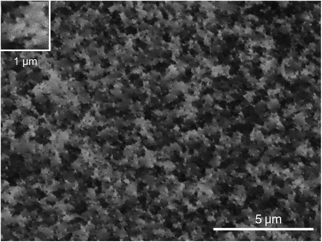
Figure 1.ECCI micrograph from AlGaN thin film.
Techniques have also been developed to identify dislocation types [11,24,40]. Nitride semiconductors contain three types of TDs, namely screw-, edge-, and mixed-type dislocations. To identify the TD type, it is possible to apply the “invisibility criteria” used in transmission electron microscopy (TEM) [11]. In simple terms, dislocations are invisible in an ECCI or TEM micrograph if they do not distort the plane which diffracts the incident electron beam. The invisibility criteria are satisfied for screw dislocations where and for edge and mixed dislocations where and . is the vector normal of the diffracting plane, is the Burgers vector of the TD, and is its line direction. For ECCI, to determine an electron channeling pattern is usually acquired [11]. However, a further factor which needs to be taken into account when attempting to apply the invisibility criteria to ECCI images (and plan view TEM images), is the effect of surface relaxation on the observed defect contrast. The variation in strain due to surface relaxation around a defect can dominate the observed defect contrast [11]. For nitride semiconductor thin films, surface relaxation has a major impact on the observed TD contrast, so additional strategies have been developed to identify the TDs. As discussed above, in an ECCI micrograph TDs appear as spots exhibiting B-W contrast. If two (or more) ECCI micrographs of the same area are acquired at different diffraction conditions, the direction of the B-W contrast exhibited for each TD may be compared. If the B-W contrast direction for a given TD remains the same or is reversed, the TD is an edge dislocation. If the B-W contrast changes its direction by other than 0° or 180°, then the dislocation contains a screw component, so it is a screw or mixed TD. One advantage of this latter strategy is that it can be applied without a precise knowledge of .
For this AlGaN/GaN thin film the average TD density was determined to be . Approximately two thirds of the total TDs were found to be edge-type TDs by comparing the B-W contrast direction of the TDs for ECCI micrographs acquired under multiple diffraction conditions.
B. ECCI and EBSD Mapping of a c-plane AlN Thin Film Overgrown on a Nanopatterned Sapphire Substrate
Figure 2 shows ECCI micrographs from a thick -plane AlN thin film overgrown by MOVPE on a nanopatterned sapphire substrate (nPSS). For this sample the sapphire substrate has a 0.1° offcut toward the sapphire -plane. A hexagonal array of truncated cones was prepared on a 2-in. wafer by combining displacement Talbot lithography and lift-off to create a metal nanodot mask, followed by chlorine-based dry etching [41,42]. AlN was overgrown according to the growth process given in Ref. [43].

Figure 2.(a) SE image of nPSS, (b) schematic of overgrowth of AlN on nPSS, and (c) ECCI micrograph from an AlN thin film. Inset is on the same scale but with higher resolution.
The motivation for the growth of AlN on nPSS is to produce high-quality (low dislocation density) AlN/sapphire templates for the manufacture of high-performance UV LEDs. The reduction of dislocation densities from to has been shown to improve the internal quantum efficiency of UV LED structures from to [44].
Figure 2(a) shows a secondary electron (SE) of the nPSS and Fig. 2(b) shows a schematic of the cross section of the desired AlN overgrowth. The ECCI micrographs shown in Fig. 2(c) of the AlN/nPSS were acquired at an electron beam energy of 25 keV using the Quanta SEM operated in low vacuum mode (0.5 mbar) to avoid charging of this insulating specimen.
The variation in gray scale in the ECCI micrograph of Fig. 2(c) is a result of small differences in orientation of sub-grains in the thin film. The inset (same scale) shows a higher-resolution ECCI micrograph where threading dislocations propagating to the surface of the sample are also revealed. A significant number of the TDs are located on the sub-grain boundaries. The TDs which line up along a given sub-grain boundary all exhibit the same direction of black-white contrast (perpendicular to the sub-grain boundary); this is consistent with them being edge dislocations aligned along a low-angle grain boundary [45]. For this sample the average TD density was determined to be . Approximately 90% of the TDs were found to be edge-type TDs by comparing the B-W contrast direction of the TDs for ECCI micrographs acquired under multiple diffraction conditions.
As discussed in the previous section, while ECCI reveals misorientations between sub-grains, it does not provide a measure of the magnitudes and directions of the misorientations. To obtain quantitative information, EBSD data were acquired from the same sample at an electron beam energy of 20 keV using the Quanta SEM again in low vacuum mode. Figure 3(a) shows a grain reference orientation deviation (GROD) map (the deviation of orientation of the sub-grains relative to an average orientation [46]) derived from EBSD data using MTEX [47]. The first step of the analysis involved comparison of each EBSP with dynamical simulations [48]. Figure 3(b) is a GROD angle map which shows the local misorientations relative to the normal to the sample, i.e., the -axis ([0001] direction) and reveals that the local misorientations are predominantly rotations around the -axis. As shown schematically in Fig. 3(b), the colors, blue and red, denote the direction of in-plane rotation. The red regions are rotated in the opposite direction to the blue regions. Work is ongoing to determine the origin of the observed sub-grain rotations, but it is most likely related to the mismatch between the AlN layer and its substrate and to the misfit dislocations which form to accommodate the mismatch [49].
Figure 3.EBSD maps from the AlN/nPSS thin film: (a) grain reference orientation deviation (GROD) map and (b) GROD axis map relative to the sample normal (c-axis, [0001] direction]) where the colors denote direction of in-plane rotation (i.e., around the c-axis). The red regions are rotated in the opposite direction to the blue regions as indicated.
These results illustrate how ECCI and EBSD can provide complementary structural information. ECCI allows fast determination of dislocation densities and their distribution and reveals the presence of sub-grains; Fig. 1 took around 10 min of direct acquisition. EBSD provides quantitative information on the magnitude and direction of the misorientations in the film. However, the EBSD data from which the maps of Fig. 3 were derived, took of order 3 h to acquire. The EBSD data acquisition was then followed by further data analysis which is also time consuming. The time required to acquire the EBSD data can result in drift and in this case a number of datasets were acquired before one was obtained which was relatively drift free. Note that a slight drift can be seen within the top micrometer of the maps shown in Fig. 3. In spite of this, both techniques share the advantages of being non-destructive and can be used to interrogate large areas of a sample.
C. CL Imaging and ECCI of a Semi-Polar (11-22) GaN Thin Film Overgrown on GaN Microrods on m-Sapphire
UV LEDs produced from semi-polar nitride semiconductor thin films promise higher performance than those produced from their polar counterparts, due to reduction of piezoelectric and spontaneous polarization fields. Unfortunately, semi-polar nitride semiconductor thin films are often of poor quality with a high density of structural defects; in particular stacking faults, in addition to threading dislocations [50–54]. Here we report the study of the structural and luminescence properties of a 5 μm thick (11-22) GaN epilayer overgrown by MOVPE on a regular array of microrods on an -plane sapphire substrate using ECCI and room temperature CL imaging. The microrod template and overgrowth is designed to reduce the density of structural defects through overgrowth initiated from the sidewalls of the microrods and exploitation of the faster growth rate in the -direction compared to the - and -plane directions to block the propagation of defects; for more information see Ref. [53]. Figure 4(a) shows a schematic of the structure and illustrates that the growth gives rise to alternating striped regions, where stacking faults reach the surface of the sample or no stacking faults are present, respectively. Figures 4(b) and 4(d) show an ECCI micrograph and integrated CL intensity image of the GaN near band edge (NBE) emission (3.15–3.50 eV), respectively, from a sample where a semi-polar (11-22) GaN thin film was overgrown on 5 μm diameter GaN microrods. These images are plotted on the same scale but were not obtained from the same part of the sample. The ECCI micrograph was acquired at an electron beam energy of 30 keV in the Sirion SEM while the CL image was acquired at an electron beam energy of 5 keV. The ECCI micrograph of Fig. 4(b) reveals that the GaN thin film does indeed exhibit striped regions of high stacking fault density separated by regions with almost no stacking faults. The average stacking fault density in the high stacking fault density regions is estimated to be of order . The NBE CL image of Fig. 4(d) shows alternating bright and dark stripes; we attribute the significant reduction in the NBE luminescence intensity in the dark striped regions to non-radiative recombination at the stacking faults. Figure 4(c) shows example CL spectra from a bright stripe and from a dark stripe, respectively [the boxes in Fig. 4(d) indicate where the spectra were extracted from the CL dataset], and shows that the peak intensity of the NBE peak drops by around an order of magnitude in the dark striped regions compared to the bright striped regions. At low temperature, distinctive luminescence peaks associated with stacking faults are generally observed [55–57]. However, the intensities of these peaks reduce significantly as the temperature is increased and are difficult to resolve from the broad free exciton peak at room temperature. As our CL maps have been acquired at room temperature, the dominant effect of the presence of stacking faults is a reduction in luminescence intensity.
Figure 4.(a) Schematic of semi-polar GaN microrod template and overgrowth, indicating the distribution of stacking faults on the surface of the sample and the crystallographic directions. (b) ECCI micrograph revealing stacking faults. (c) Example CL spectra from a dark stripe and a bright stripe, respectively. The boxes on (d) indicate where the spectra were extracted from the CL dataset. (d) Integrated CL intensity image of the GaN near band edge (NBE) emission (3.15–3.50 eV) on the same scale as (e) but not from the same area. (e) Higher resolution ECCI micrograph revealing dislocations. (f) Integrated CL intensity image of the GaN near band edge (NBE) emission (3.15–3.50 eV) on the same scale as (e) but not from the same area.
Figures 4(e) and 4(f) show a higher magnification ECCI micrograph and a higher magnification CL map, respectively (same scale, not the same part of the sample). The ECCI micrograph reveals striped regions with alternating higher and lower dislocation densities. By changing the tilt and rotation of the sample, diffraction conditions can be selected to provide the strongest contrast for the stacking faults or for the dislocations.
The dislocation density in the high-density regions is , while for the lower-density region it is [58]. We attribute the black spots in the CL images of Figs. 4(d) and 4(f) to single or clusters of dislocations.
In summary, comparison of the ECCI micrographs with the CL images shows that at room temperature, both stacking faults and dislocations lead to a significant reduction in the NBE luminescence intensity due to non-radiative recombination at these defects.
D. ECCI and CL Hyperspectral Mapping of a c-plane Si-Doped Thin Film Grown on a Stripe Patterned Epitaxially Laterally Overgrown AlN/Sapphire Template
The topography, type and distribution of dislocations, and light emission were investigated for a polar (-plane) Si-doped thin film grown on a stripe patterned epitaxially laterally overgrown (ELO) AlN/sapphire template [31]. Both the template and thin film were grown by MOVPE. The stripe pattern comprised 2 μm wide stripes (seed regions), separated by 1 μm wide grooves (window regions), running perpendicularly to the substrate miscut of toward the sapphire -plane (1-100). Note that the sapphire -plane is perpendicular to AlN -plane so that the stripes run parallel to the [1-100] direction for the ELO AlN and for any subsequently grown nitride layers. More details on the template growth can be found in Ref. [59]. For the sample we report on here, the template was overgrown by a 400 nm thick AlN buffer layer followed by a 25 nm thick graded transition layer and a 100 nm thick non-intentionally doped layer. Finally, a 1600 nm thick Si-doped layer was grown. The average percentage of AlN was determined to be by high-resolution X-ray diffraction and WDX, and the Si-dopant concentration was estimated by WDX to be [31].
Figure 5(a) shows a schematic of the sample structure. Figure 5(b) is an atomic force microscopy image of the sample, revealing the hillock morphology of the sample. Figure 5(c) is an ECCI micrograph, Fig. 5(e) is a backscattered electron topographic image; a small rotation of the sample from the orientation at which the ECCI micrograph was acquired results in topographic rather than diffraction contrast dominating the image, so revealing the hillock morphology of the sample. Figure 5(d) is a CL peak intensity image of the AlGaN NBE emission () and Fig. 5(f) is a CL peak energy image of the AlGaN NBE emission. The ECCI micrograph and topographic image were acquired at an energy of 30 keV in the Sirion SEM, while the CL maps were acquired at an energy of 5 keV using the Quanta SEM. As these samples were conducting as a result of the silicon doping, both types of measurements could be made in the standard high vacuum mode. For a detailed discussion of the CL spectroscopy of this sample, see Ref. [31]. Images in Figs. 5(c)–5(f) were obtained from approximately the same region of the sample. The white arrows indicate the apexes of the hillocks. Complete alignment of these images was not possible as the images were acquired at different sample tilts and rotations. The sample was tilted at 70° from the incident electron beam direction for the ECCI and backscattered electron topographic image, with a small rotation between the ECCI and topographic images, and it was tilted at 45° for the CL images.
Figure 5.(a) Schematic of the sample structure. for the top 1.6 μm layer. (b) Atomic force microscopy image of the sample surface. (c) ECCI micrograph (the black brackets indicate “stripes” of higher dislocation density in the coalescence region). (d) Topographic image. (c) CL near band edge (NBE) peak intensity map. (d) NBE CL peak energy map. Images (c) to (f) were acquired from approximately the same region of the sample. The white arrows indicate the apexes of the hillocks. The CL peak intensity and peak energy were extracted from hyperspectral data.
The ECCI micrograph reveals that the patterned template leads to a modulation of the dislocation density with higher dislocation densities around the ELO coalescence boundaries. Analysis reveals an average TD density of , with a density of around the coalescence boundaries and a dislocation density of in the lower dislocation regions. 97% of the dislocations were found to be edge-type dislocations. High-resolution ECCI micrographs (not shown here) show that the dislocations at the coalescence boundaries are arranged in lines with the same direction of black-white contrast (perpendicular to the coalescence boundary), in a similar manner to the rotation boundaries observed for the AlN thin film described in Section 3.B. This observation is consistent with coalescence giving rise to low-angle grain boundaries.
Comparison of the ECCI micrograph of Fig. 5(c) and the topographic image of Fig. 5(e) shows that threading dislocations with a screw component are located at the apex of each hillock. The ECCI micrograph also shows atomic steps around the hillocks. This hillock morphology is a result of spiral growth around the screw component dislocations [60–62].
Comparing the ECCI micrograph with the CL NBE peak intensity image in Fig. 5(d) reveals that the presence of dislocations leads to a reduction in the luminescence; in particular, dislocations with a screw component appear as dark spots in the CL image.
Comparing Figs. 5(e) and 5(f) shows that the NBE emission is redshifted at the edges of the hillocks. The AlGaN peak energy is dependent on the relative percentages of GaN and AlN in the AlGaN thin film, the lower the energy of the NBE emission, the higher the percentage of GaN in the film. The peak position will also be influenced by strain and by doping density.
The origin of the redshift will be the subject of further study, for example, WDX mapping experiments (as described in the next section for a similar sample) could allow changes in the fractions of AlN and GaN to be mapped.
E. Composition and Doping in AlGaN
WDX analysis allows the straightforward and non-destructive analysis of both major and minor elements in surface layers with thicknesses typically greater than approximately 100 nm [63,64]. Here we describe mapping of the AlN and GaN content across topographic surface features in MOVPE grown AlGaN epilayers, as well as measurement of the concentration of Si-dopants in GaN epilayers, using a comparison with secondary ion mass spectrometry (SIMS) data. A calibration curve method is described, allowing the WDX data to be converted to doping densities in the range .
The AlGaN layers were mapped in the JEOL EPMA, using an acceleration voltage of 15 kV and a beam current of 40 nA, by stepping the sample underneath a focused electron beam at normal incidence and using individual spectrometers to measure the intensities of Ga , Al , and N X-rays at each point. The AlN and GaN mole fractions can be accurately quantified with the WDX correction routines. Composition maps were generated as shown for Ga and Al in Figs. 6(a) and 6(c), respectively, either side of the backscattered electron (BSE) image [Fig. 6(b)] of the mapped region. The BSE image reveals a surface morphology of neighboring platelet-like structures. The WDX measurements revealed that the average AlN content was 81% for this layer. The maps of Fig. 6 show opposing behavior for the AlN and GaN mole fractions, with the Ga signal lower at the center of the platelets relative to the edges, while the Al signal is lower at the edges relative to the center.
Figure 6.WDX maps of the intensities of (a) Ga (left) and (c) Al (right) X-rays, and (b) a backscattered electron image (center) of a micrometer-scale region of a c-plane AlGaN sample, with an average AlN content of 81%. The scale bar for X-ray intensities applies to both WDX maps, although with different absolute values.
A range of Si-doped GaN epilayers grown by MOVPE were investigated, with thicknesses in excess of 500 nm. WDX measurements were performed in the JEOL EPMA, using an acceleration voltage of 10 kV and a beam current of 40 nA for the major elements. The current (400 nA) and counting time are increased considerably for measurement of the trace elements (Si) in order to maximize the statistical accuracy. SIMS data were available from a small subset of these. At this acceleration voltage, 90% of the beam energy is deposited in the first 460 nm of a GaN sample, according to Monte Carlo simulations using the CASINO software [65]. The Ga and Si X-ray intensities were recorded using large thallium acid phthalate (TAP) crystals while for the N signal a synthetic layered crystal (LDE1L) was used. The peak-minus-background signals were compared with those measured from GaN and pure Si standards under the same conditions, to give the experimental k-ratios (sample intensity/standard intensity). The measured k-ratios can be converted to atomic percentages using iterative correction routines [63]. The values reported in Ref. [63] were observed to increase with the intensity of the Si X-rays, but appear to be on the high side, and work continues to establish the reasons why. In the meantime, we describe here how a calibration curve method can be used to quantify the Si content.
Figure 7(a) plots the Si concentration determined from SIMS against the measured WDX Si peak intensity. The samples for which SIMS data was obtained are indicated by the red points. A semi-log plot is used to separate the data points from samples with lower WDX Si peak intensities, with the intensity of the Si peak increasing with the Si concentration. The black data points then show the WDX Si peak intensity measured for all the Si:GaN samples and the Si concentration can then be read from the graph.
Figure 7.(a) Semi-log plot showing the measured Si content in the GaN layers, calibrated using the points where SIMS data is available (red data points). (b) Long qualitative scan for Si for the sample with lowest measured Si content , using a TAP crystal showing the WDX Si peak.
Figure 7(b) shows a WDX spectrum in the region of the Si line obtained with the large TAP crystal for a sample with Si, showing how the Si peak remains clearly visible above the background. By using appropriate conditions, concentrations of the order of 10 ppm (parts per million) of Si ( Si in GaN) are detectable in favorable cases, with the ultimate detection limit close to 1 ppm ( Si in GaN).
4. SUMMARY AND CONCLUSIONS
In summary, we have illustrated the capabilities of a range of non-destructive SEM techniques that can be used to provide complementary information on material properties encompassing topography, structure, composition, and light emission down to the nanoscale. Recent general availability of environmental/variable pressure SEMs has made the characterization of wide bandgap and therefore resistive materials such as AlN and AlGaN in the SEM far more accessible. We have shown that EBSD and ECCI can provide valuable information on misorientations and on extended defects, such as dislocations and stacking faults. We have also shown that WDX can be used to investigate both composition and doping in nitride semiconductor layers. If ECCI is combined with CL, the influence of extended defects on light emission can be investigated. In conclusion the SEM is a very useful tool to investigate UV-emitting nitride semiconductor thin films. The data associated with all figures in this paper may be accessed [66].
Acknowledgment
Acknowledgment. The authors would like to acknowledge financial support of the Engineering and Physical Sciences Research Council, UK via Grant No. EP/J015792/1, “Nanoscale characterisation of nitride semiconductor thin films using EBSD, ECCI, CL and EBIC”; Grant No. EP/M015181/1, “Manufacturing nano-engineered III-nitrides”; and Grant No. EP/P015719/1, “Quantitative non-destructive nanoscale characterisation of advanced materials”. Work at Ferdinand-Braun-Institute and TU Berlin was partially supported by the German “Federal Ministry of Education and Research” (BMBF) within the “Advanced UV for Life” consortium and the “German Research Foundation” (DFG) within the “Collaborative Research Center 787”.
References
[1] D. B. Holt, D. C. Joy. SEM Microcharacterization of Semiconductors(1989).
[2] J. Goldstein, D. Newbury, D. Joy, C. Lyman, P. Echlin, E. Lifshin, L. Sawyer, J. Michael. Scanning Electron Microscopy and X-ray Microanalysis(2007).
[3] L. Reimer. Scanning Electron Microscopy: Physics of Image Formation and Microanalysis(1998).
[4] W. Zhou, Z. L. Wang. Scanning Microscopy for Nanotechnology: Techniques and Applications(2007).
[5] A. J. Schwartz, M. Kumar, B. L. Adams, D. P. Field. Electron Backscatter Diffraction in Materials Science(2009).
[6] A. J. Wilkinson, P. B. Hirsch. Electron diffraction based techniques in scanning electron microscopy of bulk materials. Micron, 28, 279-308(1997).
[7] A. J. Wilkinson, T. B. Britton. Strains, planes, and EBSD in materials science. Mater. Today, 15, 366-376(2012).
[8] C. Trager-Cowan, F. Sweeney, P. W. Trimby, A. P. Day, A. Gholinia, N.-H. Schmidt, P. J. Parbrook, A. J. Wilkinson, I. M. Watson. Electron backscatter diffraction and electron channeling contrast imaging of tilt and dislocations in nitride thin films. Phys. Rev. B, 75, 085301(2007).
[9] M. A. Crimp, B. A. Simkin, B. C. Ng. Demonstration of the g·bxu=0 edge dislocation invisibility criterion for electron channelling contrast imaging. Philos. Mag. Lett., 81, 833-837(2001).
[10] Y. Picard, R. Kamaladasa, M. De Graef, N. Nuhfer, W. Mershon, T. Owens, L. Sedlacek, F. Lopour. Future prospects for defect and strain analysis in the SEM via electron channeling. Microsc. Today, 20, 12-16(2012).
[11] G. Naresh-Kumar, B. Hourahine, P. R. Edwards, A. P. Day, A. Winkelmann, A. J. Wilkinson, P. J. Parbrook, G. England, C. Trager-Cowan. Rapid nondestructive analysis of threading dislocations in wurtzite materials using the scanning electron microscope. Phys. Rev. Lett., 108, 135503(2012).
[12] S. Zaefferer, N. N. Elhami. Theory and application of electron channelling contrast imaging under controlled diffraction conditions. Acta Mater., 75, 20-50(2014).
[13] J. I. Deitz, S. D. Carnevale, S. A. Ringel, D. W. McComb, T. J. Grassman. Electron channeling contrast imaging for rapid III-V heteroepitaxial characterization. J. Vis. Exp., 101, e52745(2015).
[14] G. Naresh-Kumar, D. Thomson, M. Nouf-Allehiani, J. Bruckbauer, P. R. Edwards, B. Hourahine, R. W. Martin, C. Trager-Cowan. Electron channelling contrast imaging for III-nitride thin film structures. Mater. Sci. Semicond. Process., 47, 44-50(2016).
[15] B. G. Yacobi, D. B. Holt. Cathodoluminescence Microscopy of Inorganic Solids(1990).
[16] P. R. Edwards, R. W. Martin. Cathodoluminescence nano-characterization of semiconductors. Semicond. Sci. Technol., 26, 064005(2011).
[17] E. B. Yakimov. Investigation of electrical and optical properties in semiconductor structures via SEM techniques with high spatial resolution. J. Surf. Invest.: X-Ray, Synchrotron Neutron Tech., 6, 887-889(2012).
[18] https://www.ifkp.tu-berlin.de/fileadmin/i1/Kneissl/EQE_20181120.pdf. https://www.ifkp.tu-berlin.de/fileadmin/i1/Kneissl/EQE_20181120.pdf
[19] J. S. Park, J. K. Kim, J. Cho, T. Y. Seong. Group III-nitride-based ultraviolet light-emitting diodes: ways of increasing external quantum efficiency. ECS J. Solid State Sci. Technol., 6, Q42-Q52(2017).
[20] A. J. Wilkinson, G. Meaden, D. J. Dingley. High-resolution elastic strain measurement from electron backscatter diffraction patterns: new levels of sensitivity. Ultramicroscopy, 106, 307-313(2006).
[21] G. Naresh-Kumar, A. Vilalta-Clemente, H. Jussila, A. Winkelmann, G. Nolze, S. Vespucci, S. Nagarajan, A. J. Wilkinson, C. Trager-Cowan. Quantitative imaging of anti-phase domains by polarity sensitive orientation mapping using electron backscatter diffraction. Sci. Rep., 7, 10916(2017).
[22] E. A. Holm, A. Winkelmann, S. Farjami, G. Nolze, M. Himmerlich, P. Manohar, V. Lebedev, G. Rohrer, A. Reichmann, A. D. Rollett, D. Srolovitz, H. Weiland. Point-group sensitive orientation mapping using EBSD. Proceedings of the 6th International Conference on Recrystallization and Grain Growth, 281-286(2016).
[23] G. Naresh-Kumar, C. Mauder, K. R. Wang, S. Kraeusel, J. Bruckbauer, P. R. Edwards, B. Hourahine, H. Kalisch, A. Vescan, C. Giesen, M. Heuken. Electron channeling contrast imaging studies of nonpolar nitrides using a scanning electron microscope. Appl. Phys. Lett., 102, 142103(2013).
[24] S. D. Carnevale, J. I. Deitz, J. A. Carlin, Y. N. Picard, M. De Graef, S. A. Ringel, T. J. Grassman. Rapid misfit dislocation characterization in heteroepitaxial III-V/Si thin films by electron channeling contrast imaging. Appl. Phys. Lett., 104, 232111(2014).
[25] J. K. Hite, M. A. Mastro, C. R. Eddy. Approach for dislocation free GaN epitaxy. J. Cryst. Growth, 312, 3143-3146(2010).
[26] A. Schulze, L. Strakos, T. Vystavel, R. Loo, A. Pacco, N. Collaert, W. Vandervost, M. Caymax. Non-destructive characterization of extended crystalline defects in confined semiconductor device structures. Nanoscale, 10, 7058-7066(2018).
[27] P. G. Callahan, B. B. Haidet, D. Jung, G. G. Seward, K. Mukherjee. Direct observation of recombination-enhanced dislocation glide in heteroepitaxial GaAs on silicon. Phys. Rev. Mater., 2, 081601(2018).
[28] K. N. Yaung, S. Kirnstoetter, J. Faucher, A. Gerger, A. Lochtefeld, A. Barnett, L. L. Minjoo. Threading dislocation density characterization in III-V photovoltaic materials by electron channeling contrast imaging. J. Cryst. Growth, 453, 65-70(2016).
[29] H. G. J. Moseley. The high-frequency spectra of the elements. Philos. Mag., 27, 703-713(1914).
[30] J. J. Friel, C. E. Lyman. X-ray mapping in electron-beam instruments. Microsc. Microanal., 12, 2-5(2006).
[31] G. Kusch, M. Nouf-Allehiani, F. Mehnke, C. Kuhn, P. R. Edwards, T. Wernicke, A. Knauer, V. Kueller, G. Naresh-Kumar, M. Weyers, M. Kneissl. Spatial clustering of defect luminescence centers in Si-doped low resistivity Al0.82Ga0. 18N. Appl. Phys. Lett., 107, 072103(2015).
[32] G. Naresh-Kumar, J. Bruckbauer, P. R. Edwards, S. Kraeusel, B. Hourahine, R. W. Martin, M. J. Kappers, M. A. Moram, S. Loveloc, R. A. Oliver, C. J. Humphreys. Coincident electron channeling and cathodoluminescence studies of threading dislocations in GaN. Microsc. Microanal., 20, 55-60(2014).
[33] J. Bruckbauer, P. R. Edwards, T. Wang, R. W. Martin. High resolution cathodoluminescence hyperspectral imaging of surface features in InGaN/GaN multiple quantum well structures. Appl. Phys. Lett., 98, 141908(2011).
[34] C. E. Norman. Challenging the spatial resolution limits of CL and EBIC. Solid State Phenom., 78, 19-28(2001).
[35] J. Christen, M. Grundmann, D. Bimberg. Scanning cathodoluminescence microscopy—a unique approach to atomic-scale characterization of heterointerfaces and imaging of semiconductor inhomogeneities. J. Vac. Sci. Technol. B, 9, 2358-2368(1991).
[36] G. Kusch, H. Li, P. R. Edwards, J. Bruckbauer, P. J. Parbrook, R. W. Martin. Influence of substrate miscut angle on surface morphology and luminescence properties of AlGaN. Appl. Phys. Lett., 104, 092114(2014).
[37] M. D. Smith, D. Thomson, V. Z. Zubialevich, H. Li, G. Naresh-Kumar, C. Trager-Cowan, P. J. Parbrook. Nanoscale fissure formation in AlxGa1–xN/GaN heterostructures and their influence on ohmic contact formation. Phys. Status Solidi A, 214, 1600353(2017).
[38] E. Pascal, B. Hourahine, G. Naresh-Kumar, K. Mingard, C. Trager-Cowan. Dislocation contrast in electron channelling contrast images as projections of strain-like components. Mater. Today, 5, 14652-14661(2018).
[39] A. P. Day, T. E. Quested. A comparison of grain imaging and measurement using horizontal orientation and colour orientation contrast imaging, electron backscatter pattern and optical methods. J. Microsc., 195, 186-196(1999).
[40] R. J. Kamaladasa, F. Liu, L. M. Porter, R. F. Davis, D. D. Koleske, G. Mulholland, K. A. Jones, Y. N. Picard. Identifying threading dislocations in GaN films and substrates by electron channeling. J. Microsc., 244, 311-319(2011).
[41] P. M. Coulon, G. Kusch, P. Fletcher, P. Chausse, R. W. Martin, P. Shields. Hybrid top-down/bottom-up fabrication of a highly uniform and organized faceted AlN nanorod scaffold. Materials, 11, 1140(2018).
[42] P. M. Coulon, B. Damilano, B. Alloing, P. Chausse, S. Walde, J. Enslin, R. Armstrong, S. Vézian, S. Hagedorn, T. Wernicke, J. Massies, J. Zúñiga‐Pérez, M. Weyers, M. Kneissl, P. A. Shields. Displacement Talbot lithography for nano-engineering of III-nitride materials. Microsyst. Nanoeng.,(2019).
[43] S. Hagedorn, A. Knauer, A. Mogilatenko, E. Richter, M. Weyers. AlN growth on nano-patterned sapphire: a route for cost efficient pseudo substrates for deep UV LEDs. Phys. Status Solidi A, 213, 3178-3185(2016).
[44] M. Kneissl, T. Y. Seong, J. Han, H. Amano. The emergence and prospects of deep-ultraviolet light-emitting diode technologies. Nat. Photonics., 13, 233-244(2019).
[45] V. Potin, P. Ruterana, G. Nouet, R. C. Pond, H. Morkoç. Mosaic growth of GaN on (0001) sapphire: a high-resolution electron microscopy and crystallographic study of threading dislocations from low-angle to high-angle grain boundaries. Phys. Rev. B, 61, 5587-5599(2000).
[46] S. I. Wright, M. M. Nowell, D. P. Field. A review of strain analysis using electron backscatter diffraction. Microsc. Microanal., 17, 316-329(2011).
[47] F. Bachmann, R. Hielscher, H. Schaeben. Texture analysis with MTEX–free and open source software toolbox. Solid State Phenom., 160, 63-68(2010).
[48] A. Winkelmann, C. Trager-Cowan, F. Sweeney, A. P. Day, P. J. Parbrook. Many-beam dynamical simulation of electron backscatter diffraction patterns. Ultramicroscopy, 107, 414-421(2007).
[49] N. Mante, S. Rennesson, E. Frayssinet, L. Largeau, F. Semond, J. L. Rouviere, G. Feuillet, P. Vennéguès. Proposition of a model elucidating the AlN-on-Si (111) microstructure. J. Appl. Phys., 123, 215701(2018).
[50] R. Mantach, P. Vennéguès, J. Z. Perez, P. De Mierry, M. Leroux, M. Portail, G. Feuillet. Semipolar (10-11) GaN growth on silicon-on-insulator substrates: defect reduction and meltback etching suppression. J. Appl. Phys., 125, 035703(2019).
[51] B. Leung, D. Wang, Y. S. Kuo, J. Han. Complete orientational access for semipolar GaN devices on sapphire. Phys. Status Solidi B, 253, 23-35(2016).
[52] F. Scholz. Semipolar GaN grown on foreign substrates: a review. Semicond. Sci. Technol., 27, 024002(2012).
[53] Y. Zhang, J. Bai, Y. Hou, X. Yu, Y. Gong, R. M. Smith, T. Wang. Microstructure investigation of semi-polar (11-22) GaN overgrown on differently designed micro-rod array templates. Appl. Phys. Lett., 109, 241906(2016).
[54] J. Bruckbauer, Z. Li, G. Naresh-Kumar, M. Warzecha, P. R. Edwards, L. Jiu, Y. Gong, J. Bai, T. Wang, C. Trager-Cowan, R. W. Martin. Spatially-resolved optical and structural properties of semi-polar (11-22) AlxGa1–xN with x up to 0.56. Sci. Rep., 7, 10804(2017).
[55] Emission properties of a-plane GaN grown by metal-organic chemical-vapor deposition. J. Appl. Phys., 98, 093519(2005).
K. P. Korona, P. P. Paskov, A. Reszka, R. Schifano, B. Monemar, M. Sobanska, T. Paskova, P. S. Perkowska, S. Figge, A. Wysmołek, D. Hommel, K. Klosek, Z. R. Zytkiewicz. Dynamics of stacking faults luminescence in GaN/Si nanowires. J. Lumin., 155, 293-297(2014).
[57] J. Lähnemann, U. Jahn, O. Brandt, T. Flissikowski, P. Dogan, H. T. Grahn. Luminescence associated with stacking faults in GaN. J. Phys. D, 47, 423001(2014).
[58] G. Naresh-Kumar, D. Thomson, Y. Zhang, J. Bai, L. Jiu, X. Yu, Y. P. Gong, R. M. Smith, T. Wang, C. Trager-Cowan. Imaging basal plane stacking faults and dislocations in (11-22) GaN using electron channelling contrast imaging. J. Appl. Phys., 124, 065301(2018).
[59] I. Bryan, A. Mogilatenko, Z. Bryan, V. Küller, A. Knauer, S. Mita, J. Jeschke, A. Rice, L. Hussey, U. Zeimer, C. Shelton, M. Weyers, G. Tränkle, J. Tweedie, J. P. Maria, R. Collazo, Z. Sitar. The role of surface kinetics on composition and quality of AlGaN. J. Cryst. Growth, 451, 65-71(2016).
Defect analysis in AlGaN layers on AlN templates obtained by epitaxial lateral overgrowth. J. Cryst. Growth, 402, 222-229(2014).
[61] I. Bryan, Z. Bryan, S. Mita, A. Rice, J. Tweedie, R. Collazo, Z. Sitar. Surface kinetics in AlN growth: a universal model for the control of surface morphology in III-nitrides. J. Cryst. Growth, 438, 81-89(2016).
[62] L. Schade, T. Wernicke, J. Raß, S. Ploch, M. Weyers, M. Kneissl, U. T. Schwarz. Surface topology caused by dislocations in polar, semipolar, and nonpolar InGaN/GaN heterostructures. Phys. Status Solidi A, 211, 756-760(2014).
[63] G. Kusch, F. Mehnke, J. Enslin, P. R. Edwards, T. Wernicke, M. Kneissl, R. W. Martin. Analysis of doping concentration and composition in wide bandgap AlGaN: Si by wavelength dispersive x-ray spectroscopy. Semicond. Sci. Technol., 32, 035020(2017).
[64] Y. Kubo, H. Kotaro, U. Akira. Minimum detection limit and spatial resolution of thin-sample field-emission electron probe microanalysis. Ultramicroscopy, 135, 64-70(2013).
[65] D. Drouin, A. R. Couture, D. Joly, X. Tastet, V. Aimez, R. Gauvin. CASINO V2. 42—a fast and easy-to-use modeling tool for scanning electron microscopy and microanalysis users. Scanning, 29, 92-101(2007).
[66] https://doi.org/10.15129/b5238863-a088-4f30-8b13-2625260eb73a. https://doi.org/10.15129/b5238863-a088-4f30-8b13-2625260eb73a


