
Jian Luo, Qile Wu, Lin Zhou, Weixi Lu, Wenxing Yang, Jia Zhu. Plasmon-induced hot carrier dynamics and utilization[J]. Photonics Insights, 2023, 2(4): R08
- Photonics Insights
- Vol. 2, Issue 4, R08 (2023)
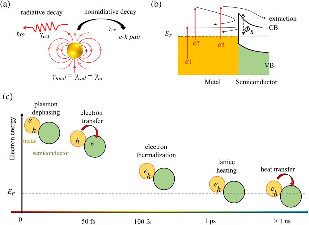
Fig. 1. (a) Schematic of the dephasing of localized surface plasmon resonance of metal nanoparticles. The total plasmon dephasing rate (
![(a) Left: schematic illustration of a typical rotating compensator ellipsometry composed of two fixed polarizers and a rotating quarter wave plate (QWP). Right: flowchart for conventional ellipsometry[72]. (b) Real (ɛ1, solid line) and imaginary (ɛ2, dashed line) parts of dielectric constant measured by ellipsometry of spin-coating Na[78], template stripped Ag film[83], single-crystal Au[73], and evaporated Cu[74]. (c) Fitted value of bulk damping rate γ (in the unit meV, τ=ℏ︀/γ) of the four metals in (b) by Drude (Ag, Au, Cu) and Drude–Lorentz (Na) models.](/richHtml/pi/2023/2/4/R08/img_002.png)
Fig. 2. (a) Left: schematic illustration of a typical rotating compensator ellipsometry composed of two fixed polarizers and a rotating quarter wave plate (QWP). Right: flowchart for conventional ellipsometry[72]. (b) Real (
Fig. 3. Calculated extinction and scattering spectra for (a), (b) Au and (c), (d) Ag nanoparticles in water (refractive index:
Fig. 4. (a) Schematic illustration of dark-field scattering technique and the relation between the line width of scattering spectra and plasmon dephasing time. (b) Line width and dephasing times of Au nanospheres and nanorods. The aspect ratios of nanorods are between two and four, and the width is about 15–20 nm[86]. (c) Contribution of electron-surf scattering and radiation damping to total plasmon damping for Au nanorods with aspect ratios between two and four and the width ranging from 8 to 30 nm[111].
Fig. 5. (a) Schematic of interference time-resolved (ITR) spectroscopy. Pump and probe pulses are at the same frequency. The detector measures the autocorrelation function (ACF) and spectral intensity (I). (b) Measured third-order ACF (solid line) of Au nanorods by ITR-THG spectroscopy. The calculated ACF (solid circles) agrees well with the experimental result with the fitting parameter dephasing time of 6 fs[118]. (c) ITR-PEEM intensity of Au nanocubes after exciting the dipole mode of LSPR. With a dephasing time of 5 fs, the simulated PEEM intensity (red line) is in good agreement with the experimental results (black line)[119]. (d) ITR-PEEM of four LSPRs on the Ag grating. The phase decay is deduced from the delay time and excitation pulse wavelength of 400 nm. The pulse width is 10 fs, so the excitation pulse has waned from 13.34 fs delay time, and the coherent polarization (0 and 6.67 fs delay time) of each dot shifts to its own resonant frequency[125].
Fig. 6. Schematic illustrations of plasmon-induced hot carriers in (a) noble metals (Au or Ag) including (A) interband transition, (B) intraband electron–electron scattering, (C) phonon-assisted intraband transition, and (D) surface-assisted collision or Landau damping; (b) non-noble plasmonic transition metals such as Fe, Co, or Ni; (c) simple metals such as Na and Al. For clarity, only the interband transition is shown in (b) and (c).
Fig. 7. Occupation ratio of four different mechanisms including direct interband transition, phonon-assisted transition, geometry-assisted transition (that is, surface damping), and resistive loss (that is, intraband electron–electron scattering) of plasmon decay in (a) bulk Au film and (b)–(d) Au NPs with diameters (
Fig. 8. Theoretical electron–hole contribution to the time-dependent electronic energy from plasmon excitation (0 fs) to dephasing (8.2 fs) of
Fig. 9. (a) Surface density of hot electrons in a nanosphere generated by LSPR damping under light irradiation. Population distribution of Drude electrons and high-energy electrons[191]. (b) Calculated local electric field enhancements of Au nanosphere, nanorod, and nanostar. Their hot electron generation rate is probed by their photocatalytic degradation rate of rhodamine B (RhB)[199]. (c) Schematic representative of the reduction of 4-ITP induced by transferred electrons from nonradiative damping of Au nanoantenna dimers. Both the hot electron generation rate and degradation rate constant of 4-ITP are proportional to the electric field enhancement that increases as gap size decreases[204].
Fig. 10. (a) Schematic illustration of increasing generation efficiency of hot electrons by narrowing the conduction band. (b) Calculated internal photoelectron conversion efficiency with the conduction band depth of 5.5 and 0.15 eV, respectively[166]. (c) Schematic illustration of sequential two plasmon excitations. The second plasmon excitation occurs before the completeness of the lattice heating induced by the first plasmon damping. (d) Time-resolved multiphoton photoluminescence (MPPL) intensity excited by IR pulse of Au nanoantenna[43].
Fig. 11. (a) Schematic illustration of the electron energy changes upon electron–electron (e-e ) and electron–phonon (e -ph) scattering. One e-e scattering event averages its energy while one e -ph scattering event has nearly no effect on electron energy but changes the direction of the electron. (b) Difference of the predicted time-dependent electron distribution from the Fermi distribution at 300 K induced by a pump pulse at 560 nm (2.2 eV)[210]. (c) Theoretical energy-dependent relaxation time (e-e and e -ph scattering in Au (upper side). Scattering rate (e-e or e -ph scattering event (lower side). The shaded area indicates the anticipation of interband transition[161].
Fig. 12. Schematic illustration of (a) plasmon-induced indirect electron transfer; (b) plasmon-induced direct electron transfer; (c) pump–probe technique probing the electron transfer.
Fig. 13. (a) FTA spectra by 3500 nm probe wavelength of three nanocrystalline films:
Fig. 14. (a) Charge density induced by DET in
Fig. 15. Promoting hot electron transfer by material design. (a) Schematic of the competition between carrier recombination and separation at the metal/semiconductor interface. (b) The photocatalytic degradation of MB by
Fig. 16. (a) Schematic illustration of the effect of external electric field on the hot electron transfer to semiconductors: lowering the Schottky barrier
Fig. 17. Schematic illustrations of (a)
Fig. 18. (a) Schematic illustration of plasmon-induced electron transfer in photovoltaics. (b) Energy levels and electron transfer direction of the
Fig. 19. (a) Left: schematic of the Au/SiNHs plasmonic hot electron photodetector and the electric field distribution. Right: time-dependent responses of the optimized devices operating at front-side and back-side illumination[273]. (b) Schematic illustration of Ag
Fig. 20. (a) Transient linear dichroism of a metasurface consisting of a lattice of Au symmetric nanocrosses. The first femtosecond pump pulse breaks the fourfold symmetry by generating hot carriers, and then a second femtosecond probe pulse with a time delay of 100 fs shows the dichroism dependent on the polarization of the pump pulse[377]. (b) Ultrafast all-optical control of the polarization of light by Au array/ITO/Au film/silicon substrate. A femtosecond pulse excites plasmonic crystal mode and triggers hot electron injection into ITO, changing its polarization response[378].
|
Table 1. Dephasing Time of Nanostructured Metallic Plasmons.
|
Table 2. Photocatalysis Based on Plasmon-Induced Hot Electron Transfer.
|
Table 3. Photovoltaics Based on Plasmon-Induced Hot Electron Transfer.
|
Table 4. Photodetectors Based on Plasmon-Induced Hot Electron Transfer.

Set citation alerts for the article
Please enter your email address
© Copyright 2018-2021 | Chinese Laser Press. All Rights Reserved 沪ICP备15018463号-20