
Jian Luo, Qile Wu, Lin Zhou, Weixi Lu, Wenxing Yang, Jia Zhu. Plasmon-induced hot carrier dynamics and utilization[J]. Photonics Insights, 2023, 2(4): R08
- Photonics Insights
- Vol. 2, Issue 4, R08 (2023)
Abstract
1 Introduction
Plasmonics, involving the collective oscillations of free electrons in metallic nanostructures and nanoparticles (NPs), has become one of the most intensively explored subfields of nanophotonics and nanooptics in the past decades. The unique property of plasmonic nanostructures to concentrate electromagnetic energy into nanoscale offers the capability for ultimate spatiotemporal light control, which has been widely applied in areas ranging from photophysics to chemistry, biology, optical engineering, as well as environmental sciences and solar energy conversion[1,2]. Compared to conventional semiconductors and organic polymers, much higher light concentration of plasmonic nanostructures provides the foundation for efficient light utilization that is critical for photochemistry, photovoltaics, optical modulation, etc.
Surface plasmons (SPs) are collective charge-density oscillations at the surface of a conducting material with high sensitivity to the properties of the plasmonic material and surrounding medium. From the viewpoint of classical electrodynamics, conduction electrons in metals are widely regarded as free electron gas or analogous to plasma. In response to an external electric field of incident light, the electrons in this plasma can travel freely throughout the metal and finally establish intrinsic oscillation at certain quantized frequencies. These quantized oscillations are called plasmons[3,4]. Basically, the plasma frequency of a bulk material is an inherent property and related to the dielectric constant of the material. In contrast, the plasma frequency of a metallic NP is highly dependent on the size and shape of the NP, as well as the surrounding dielectric environment. The oscillating electric field of incident light creates an instantaneous build-up and depletion of electrons on two sides of the NP concerning the polarization of light, creating an internal electric field that is responsible for enhanced absorption and scattering cross-sections[5]. The resonance conditions of NPs can be calculated by solving Maxwell’s equations either analytically or numerically. For lowest-order approximation with merely dipole–dipole interactions involved, the SP resonance occurs when , where is the real component of the complex dielectric constant of the bulk metal and is the dielectric constant of the medium[6]. The factor accounts for the shape of the NP. is assigned to two for a spherical particle, which reaches up to 20 or even larger for nanorods with high aspect ratios[5]. In the resonance condition, the magnitude of the electron oscillation is maximized. Thus, the internal electric field inside the NP reaches the maximum, as well as the dipolar field exterior to the NP, leading to a strong near-field enhancement in the close vicinity of the NP surface[7]. For instance, the electric field enhancement in the gap of two Ag nanocubes is a function of the distance to the surface and can achieve a factor of [8]. Such a strong electric field near the surface permits a large enhancement of nonlinear optical processes and inspires versatile applications in surface-enhanced Raman spectroscopy (SERS)[9], enhanced fluorescence sensing[10–12] and enhanced second/third harmonic generation (SHG/THG)[13].
An overview picture of the localized surface plasmon resonance (LSPR) initiated hot carrier evolution (with spatial, temporal, and energy view angles) is schematically shown in Fig. 1. Once excited by incident light, the collective oscillation of free electrons or LSPR is established instantaneously. Then the collective SP elementary excitations will lose their coherence of the collective oscillations of electrons within the sub-100 fs time scale due to the inherent plasmon damping of metals, which is also called as dephasing or decoherence process. Both radiative and nonradiative damping contribute to plasmon dephasing [Fig. 1(a)]. The radiative pathway is the light scattering wherein the absorbed photons re-emit into the far field. In contrast, nonradiative plasmon damping absorbs the photon and generates energetic electron–hole pairs. Manipulation of plasmon dephasing time is achieved by manipulating the radiative and nonradiative damping rates, which are dependent on the material, size, shape, and surrounding environment of plasmonic nanostructures and affect the line width of the absorption, scattering spectra of plasmon, as well as the generation efficiency of energetic electron–hole pairs. The ability to generate energetic electron–hole paris extends the potential applications of SPs into photocatalysis[14–18], photodetections[19,20], photovoltaics[21], and ultrafast nano-optics[22–24]. These energetic electrons and holes are called hot carriers. In general, hot electrons exhibit much longer mean free paths (MFPs) than the hot hole counterparts[25]. Therefore, explorations on hot electrons are more extensive, while investigations on hot-hole-based applications are far from hot research areas until recently[25,26]. Typically, the majority of excited electrons lie near the Fermi level (), while the highly energetic electrons possessing energy close to the absorbed photon energy are of an extremely low ratio[27].
Sign up for Photonics Insights TOC. Get the latest issue of Photonics Insights delivered right to you!Sign up now
![]()
Figure 1.(a) Schematic of the dephasing of localized surface plasmon resonance of metal nanoparticles. The total plasmon dephasing rate (
In the past decades, massive studies have been focused on the dynamics, utilization, and applications of hot electrons, and fruitful achievements have been obtained. Despite extensive efforts, the utilization efficiency of hot electrons is still far from satisfactory for practical applications. For instance, the incident photon-to-current conversion efficiencies (IPCEs) in reported solid-state photovoltaic cells based on plasmonic metal–semiconductor heterostructures are typically less than 2.5%[28–30]. The extremely low photoconversion efficiency is mainly ascribed to multiple factors, including Ohmic dissipation, ultrafast hot electron thermalization, and momentum conservation interfacial transmission[31]. These microscopic processes usually occur on a sub-picosecond time scale. A thorough understanding of hot carrier dynamics is urgently needed for rationally designing high-performance devices based on plasmon-induced hot carriers. Both sub-picosecond time resolution and nanoscale spatial accuracy are needed, demanding a combination of accurate NP fabrications, femtosecond time-resolved techniques, near-field microscopies with high spatial resolutions and solid-state theories.
A common structure to extract the plasmon-induced hot electrons in metals is the metal/semiconductor heterostructure. The metal–metal contact and metal–insulator contact are also common in scientific research and practical applications to modulate the SP resonance, optical transmission, and wave propagation[32–36]. As shown in Fig. 1(b), three necessary conditions should be considered for an efficient electron extraction process. (1) The excited hot electrons should possess a primary momentum towards the metal/semiconductor surface as well as a relatively high initial energy that should be much higher than the interfacial barrier height (). (2) Distinct energy loss of the generated hot electrons during the transport routes to the interface, which are mainly initiated by electron–electron and electron–phonon scatterings, should be effectively avoided. More specifically, taking the electron–electron scattering process for example, an arbitrary electron–electron collision commonly loses the energy of hot electrons by half, while the representative energy loss of a one-time electron–phonon scattering event is at the scale of several meV[37]. (3) The electrons reaching the semiconductors are ideally so energetic that they can successfully diffuse into the bulk rather than transfer back to metal induced by the Coulomb attraction with holes, the latter process of which severely reduces the extraction efficiency and thus finally limits the overall hot carrier utilization efficiency[38]. It is worth noting that there are extra issues beyond the three conditions mentioned above such as the electron trap and energy loss in semiconductors, which have been detailly discussed in the semiconductor-based photocatalysis field[39]. We mainly focus on the above-mentioned three issues for the efficient hot carrier utilization.
Figure 1(c) shows the characteristic time scale of plasmon-induced hot electron dynamics. Plasmon dephasing is the primary process to generate hot electrons in the sub-100 fs time scale, during which the energy distribution of the electrons is highly non-thermal. Then, energy transfer from the hot electrons into cool electrons and lattice happens initiated by electron–electron and electron–phonon scattering until a thermalized Fermi–Dirac distribution profile is established. This process, called electron thermalization, is usually completed in less than 500 fs[40,41]. After thermalization, the ratio of high-energy electrons able to surmount the Schottky barrier is usually negligible. The characteristic electron temperature is only slightly higher than the lattice temperature. Electrons are distributed in a narrow energy region near [42]. Therefore, the electron injection process should occur faster than electron thermalization. After electron thermalization, electron–phonon scattering can further contribute to the electron cooling and lattice heating until thermal equilibrium between electrons and lattice is established, which is usually completed within several picoseconds for noble metal NPs[43,44]. Finally, the heated lattice transfers the heat into an environment where the heat dissipation rate is dependent on the medium[45]. Basically, the electron–phonon scattering is widely regarded as the next step of the electron–electron scattering in most electron-dynamics-based studies, which commonly occurs at a picosecond time scale according to the two-temperature model (TTM) and its extensions[46–53]. However, it is worth noting that both the electron–electron and electron–phonon scattering events occur at the same time scale of [54]. Electron–electron scattering changes the electron energy significantly while electron–phonon scattering changes the electron energy much less but mainly the moving direction when hot electrons possess excessive energy at the optical range. Actually, electron thermalization is mainly induced by numerous electron–electron scatterings. However, a considerable amount of energy of the energetic electrons will be transferred to a lattice by the electron–phonon scatterings during the electron thermalization process, which has been evidenced in a 24 nm thick Cu film identified by Obergfell M and Demsar J[51].
There have been a couple of reviews and perspectives on the mechanism of hot electron generation[55,56], hot electron transmission[57–60], as well as hot-electron-based materials and devices[21,61,62]. In this review, we aim to provide an overall physical picture of plasmon-induced hot electron utilization via comprehensive discussions of experimental and theoretical results, as well as a brief introduction on the hot-carrier-based applications including photocatalysis, photodetectors, photovoltaics, and ultrafast nanooptics. The challenges and possible solutions in the hot electron generation and extraction are emphasized. It should be noted that besides plasmonic metals, plasmonic semiconductors including metal oxides, metal chalcogenides, metal nitrides, silicon, and other materials have come into play in recent years[63]. Due to the low density of free electrons, the plasmonic bands in semiconductors are typically in the regime from near-infrared to terahertz frequencies. The generated hot carriers possess relatively low energy. Thus, plasmonic semiconductors are mainly used as the complementing metals in plasmonics[64,65]. This review is focused on the plasmon in metals and organized as follows. The mechanisms of plasmon decay and hot electron generation are discussed in Section 2. The principles and techniques to measure plasmon dephasing time are discussed, as well as the initial energy distribution of hot carriers. Then, the strategies to increase hot electron generation efficiency are discussed in Section 3. In Section 4, the dynamics of hot carrier transfer is discussed, which includes electron transport in metals, electron injection, and charge recombination. The strategies to enhance electron transfer at the interface are given in Section 5. In Section 6, plasmon-induced hot carrier applications are briefly introduced. Finally, conclusions and prospects are given in Section 7. We suggest that this review will provide a basis and guideline for new researchers in the field of plasmon-induced hot carrier applications.
2 Dynamics of Plasmon Damping and Hot Carrier Generation
Plasmon damping or dephasing occurs via radiative and nonradiative pathways. Radiative damping is the elastic scattering that emits photons into the far field with conserved photon energy. Nonradiative damping refers to the process of light absorption. Generally, both pathways contribute to the SP damping and are competitive with each other[66]. In this section, we first give a short introduction to radiative SP damping and then discuss the hot carrier generation mechanisms in detail.
2.1 Plasmon damping of bulk metals
Before discussing the plasmon damping of metal NPs, it is essential to introduce plasmon damping of bulk metals, which represents the inherent optical loss of metals, independent of the particle size, shape, and adjacent dielectric environment. The simplest theoretical model to describe the bulk plasmon damping is the Drude model, in which the fitted damping rate of the Drude term is related to the direct-current conductivity and Ohmic loss[67]. By measuring the dielectric constants of metals, the bulk plasmon damping rates () can be retrieved. In the Drude model, conduction electrons in metals are simply treated as the free electron gas, which shows good agreement with experimental results for most simple metals such as noble metals as well as alkali metals. Featured by the collective oscillation of electrons, plasmons are modeled by a damped harmonic model. Under the relaxation time () approximation, the damping force can be expressed as , where is the effective mass of electrons, and is the distance away from the equilibrium position. Plasmon damping is regarded as a result of various electron scattering processes including electron–electron, electron–phonon, and electron–defect scattering processes: [68]. In addition, can be also expressed as where is the Fermi velocity and is the mean free path (MFP) of the electrons[69]. According to Matthiessen’s rule, , where is the MFP for the individual electron scattering process[70]. The dielectric response to an electric field induced by incident light is obtained by solving Newton’s equation of free electron motion[3,71]:
The Drude model provides a facile way to obtain via fitting frequency-dependent complex dielectric constants, which are usually measured by standard spectroscopic ellipsometry. Figure 2(a) shows the implementation of a typical rotating compensator ellipsometry composed of two fixed polarizers and a rotating quarter wave plate.[72] The sample is irradiated obliquely by - and -polarized light with incident angle , and then the complex reflection coefficient ratio is measured, where and are the incident angle-dependent changes in the amplitude ratio and phase, respectively. The key point is to construct the relationship between and , which can be obtained by either specific lineshape function fitting or deterministic theoretical analysis[72]. Figure 2(b) shows the real and imaginary components of the dielectric constants of bulk Au, Ag, Cu, and Na measured by spectroscopic ellipsometry. Based on , the bulk dephasing time can be obtained by a fitting procedure with the Drude model. Olmon et al. measured the dielectric constants of bulk Au from 690 nm to 25 µm and obtained the [73]. This lifetime is a little longer than the 9 fs measured by Johnson et al. in 1972[74]. The Fermi velocity for bulk Au is [75], indicating the MFP of electrons in bulk Au of approximately 20 nm at room temperature. For many metals, the Drude model can only give reasonable results up to optical frequencies because of interband transitions[76–78]. The onsets of the interband transitions for noble metals Au and Ag are at about 2.4 and 3.9 eV, respectively[70,79,80]. An extra term is phenomenologically added into Eq. (1) to account for the interband transitions and dielectric screening effects:
![]()
Figure 2.(a) Left: schematic illustration of a typical rotating compensator ellipsometry composed of two fixed polarizers and a rotating quarter wave plate (QWP). Right: flowchart for conventional ellipsometry[
Different expressions of have been used in the literature[77]. One of the most widely employed expressions is a sum of Lorentz terms as follows (the Drude–Lorentz model)[73,77,81,82]:
2.2 LSPR damping of metal nanoparticles characterized by line width
For the LSPR of metal NPs, there are two additional damping pathways except for the intrinsic electron scattering processes in the bulk plasmon damping: electron–surface scattering and radiation. The former pathway with the bulk electron scattering processes contributes to photon absorption while the latter mainly contributes to the scattering. Therefore, the total damping rate of a metal NP can be expressed as
In analogy to , is expressed as , where is a coefficient depending on the electron–surface interactions[85]. is the effective path length of the electrons before scattering off a surface depending on the size and shape of the NPs and can be calculated by (V: volume, S: surface area)[85]. The radiation damping rate can be calculated by , where is a coefficient characterizing the efficiency of radiation damping[86,87]. The correlation between the damping rate and dielectric constant can thus be established by substituting the bulk damping rate with in Eq. (3). Here is not included, as the radiation effect is out of the scope of the standard Drude model. Note that at optical frequencies, is valid for most plasmonic metals. Thus, one can arrive at the following simplified dielectric constant expressions from Eq. (3)[88]:
It is clearly suggested that, in the optical regime with , the real component of the dielectric constant of small particles is the same as the bulk. However, the imaginary component is distinctly modified by the introduction of an electron–surface scattering term. Note that the extra item in Eq. (5) is just a phenomenological treatment accounting for the size effect. Several theoretical works attempt to provide a microscopic explanation for surface effects using a nonlocal dielectric function[89,90].
A common method for the experimental explorations of the damping rate of metal NPs is based on the measurement of the homogenous line width (, in unit eV) of plasmon resonance. According to a damped oscillator model, the total dephasing lifetime () can be obtained from the line width based on the following expression[91]:
In the framework of standard Mie theory established in 1908[69], the extinction, scattering, and absorption cross sections () of spherical particles are obtained by solving the exact analytical solutions of Maxwell’s equation and can be expressed as
![]()
Figure 3.Calculated extinction and scattering spectra for (a), (b) Au and (c), (d) Ag nanoparticles in water (refractive index:
In the quasi-static limit, the line width of the LSPR induced by photon absorption can be calculated by[70]
For noble metals , so that
Basically, Eq. (2) works quite well for the low-frequency limit where the operation frequency is far from the interband transition region. Also, the denominator of the right side of Eq. (11) can be approximated as because the operated optical frequency is much larger than the damping rate (). By further combining with Eq. (6b), Eq. (11) can be rewritten as follows:
The total line width can then be expressed in a clear form:
Here the factor of 2 is added accounting for the -related radiation damping process [, Eq. (7)][69,86]. Equation (13) can then be rewritten as
The different dependence of electron–surface scattering and radiation damping on the particle’s dimensions makes it possible to determine the parameters and , which is important for analytic interpretations of the plasmon damping mechanisms. The surface damping is crucial for hot carrier generation (vide infra). The measured scattering spectra and line width of Au nanospheres with diameters between 20 and 150 nm and nanorods with aspect ratios ranging from two to four are in good agreement with Mie-theory-based calculations, indicating the negligible role of electron–surface scattering and radiation damping on plasmon dephasing when the width of the nanorods is 15–20 nm [Fig. 4(b)]. The relationship between plasmon resonance energy and dephasing time is contrary for nanospheres and nanorods. For nanospheres, as the particle size increases, the resonance energy is lowered and the plasmon dephasing time (1–6 fs) is decreased as the result of increased radiation damping rate by the increased volume. On the contrary, for nanorods, the plasmon dephasing time (6–20 fs) is increased as the resonance energy is lowered by an increased aspect ratio, in agreement with the EELS results that the dephasing time of Au nanorods is decreased from about 17 to 3 fs as the plasmon energy increases from 0.4 to 2.4 eV[95]. As the width range of Au nanorods is broadened to 8–30 nm, the radiation damping appears in large particles (small ) and electron–surface scattering appears in small particles (large ), as shown in Fig. 4(c)[111]. The parameter characterizing the electron–surface scattering strength is 0.37, in agreement with the results by Hubenthal et al. who used the spectral hole burning to measure the line width of Au nanorods[112]. The different dependence of electron–surface damping and radiation damping on particle dimensions makes the line width reach its minimum when is about 0.06 (width ). As the further increases, the radiation damping is negligible as evidenced by the good agreement between the measured line width and calculated [111]. As the particle sizes decrease, the scattering cross section is decreased while the absorption intensity is strengthened, making it more reasonable to measure the line width by measuring the absorption spectra. The single-particle absorption spectra of Au NPs with diameters from 33 to 5 nm were measured by PHI[98]. The resonance energy is red shifted as the NP diameter decreases and line widths of absorption spectra are broadened[98]. The experimental results are in quantitative agreement with the simulation by Mie theory using the parameter of . So far, one can find that both the resonance energy shift and spectra broadening are sensitive to particle size. As the sizes of Au nanospheres and nanorods decrease to less than about 20 nm, the electron–surface damping parameter is about 0.3 while the radiation damping is negligible, indicating the dominant role of bulk plasmon damping.
![]()
Figure 4.(a) Schematic illustration of dark-field scattering technique and the relation between the line width of scattering spectra and plasmon dephasing time. (b) Line width and dephasing times of Au nanospheres and nanorods. The aspect ratios of nanorods are between two and four, and the width is about 15–20 nm[
Besides the metal Au, the plasmon dephasing of Ag is widely investigated as well. The line width of the plasmon of the Ag nanocluster deposited on the substrate was measured to be increased from about 0.15 to 0.30 eV as the cluster diameter decreases from 12.0 to 2.0 nm by photoemission spectra, indicating the acceleration of plasmon dephasing by surface scattering[113]. The enhanced electron–surface scattering rate in small clusters decreases the dephasing time from 8.8 to 4.4 fs. The plasmon resonance energy of the Ag nanocluster is found to be inversely proportional to the diameter[113]. The homogenous line width of Ag nanorods on a sapphire substrate was measured by a spectral hole burning technique where the aspect ratio of the Ag nanorod is fixed to be 2.2 and the width varies from about 12 to 2.5 nm[114]. In this case, the resonance energy keeps at 2.9 eV. According to the calculation method of by Novo et al.[111], for Ag NPs varies from about 0.1 to 0.5. Only when increases to 0.3 does the electron–surface scattering commence, reducing the dephasing time from 6 to 5 fs.
It is worth pointing out that the primary challenges to obtain the accurate homogenous line width of plasmon resonance are always there in versatile configurations, which include the heterogeneity of the synthesized metal NPs and the measuring precision of the single-particle level detection[115,116]. Metal NPs even with the same diameter exhibit different plasmon dephasing times due to the nanometric structural difference[93,117]. For instance, El-Khoury et al. achieved hyperspectral dark-field optical microscopy by coupling a hyperspectral detector to an optical microscope[93]. They realized the spatial resolution with . By employing this technique, they measured the dephasing lifetimes of 31 Ag nanospheres with 100 nm diameter individually. The slightly inhomogeneous size and shape result in the dephasing time from 1.9 to 2.7 fs with an average of about 2.4 fs. In order to overcome the challenge, development of both a precise synthesis method of homogeneous samples and real single-particle measuring techniques is essential, the growth and obstacles of which have been reviewed by Cortes and colleagues[116]. Another way to overcome the challenge of inhomogeneous broadening is directly determining the decay time of plasmon oscillation, which requires the femtosecond time resolution techniques because of the ultrafast dephasing time. In the next section, we introduce the measurement of plasmonic field evolution by ultrafast spectroscopy.
2.3 LSPR dynamics monitored by interferometric time-resolved spectroscopy
Measuring the homogenous spectral line width can provide a simple but indirect method for determination of the plasmon dephasing rate. One direct way to monitor the plasmon damping dynamics is to measure the time evolution of a plasmonic field . According to the simple damped harmonic oscillator model, the plasmonic field intensity can be expressed as[118]
![]()
Figure 5.(a) Schematic of interference time-resolved (ITR) spectroscopy. Pump and probe pulses are at the same frequency. The detector measures the autocorrelation function (ACF) and spectral intensity (I). (b) Measured third-order ACF (solid line) of Au nanorods by ITR-THG spectroscopy. The calculated ACF (solid circles) agrees well with the experimental result with the fitting parameter dephasing time of 6 fs[
The first ITR-SHG measurement on the plasmon field decay was realized by Lamprecht et al. to study the plasmon dephasing of Ag NPs with a noncentrosymmetric shape and size of about 200 nm[120]. The dephasing times of both Ag and Au NPs are determined by fitting the experimental ACF, which is and 6 fs, respectively[121]. In order to overcome the drawback of ITR-SHG where the sample must be noncentrosymmetric, the ITR-THG technique was developed by the same research group and was used to study the plasmon dephasing of Au nanorods with a height of 14 nm and diameters ranging from 110 to 180 nm[118]. Au NPs with different aspect ratios can give rise to different optical resonances varying from 710 to 860 nm. Using a femtosecond laser with a center wavelength of 774 nm, rationally designed Au nanorod samples can achieve both resonant (extinction maximum at 774 nm) and off-resonant (extinction maximum at 860 nm) excitations. Fitting these ACFs obtains the same dephasing time of 6 fs for both [Fig. 5(b)], but the resonant excitation induces the SP field -fold stronger than non-resonant excitation. The phase difference between the driving laser pulse and plasmon field varies with time (beating) under off-resonant excitation, while it is a constant of in the resonant case. The observed beating clearly demonstrates that the nature of the plasmon is a collective coherent oscillation of plasma electrons[118]. The ITR-THG technique was also employed to study the plasmon dephasing of single Au optical antennas and found the dephasing time was only 2 fs through radiation damping, implying the efficient radiation coupling[122].
ITR-2PPE was first developed by Ogawa S and co-workers to measure the SP dephasing time of Cu(111), which is determined to be about 20 fs by measuring and fitting the ACF[123]. Compared to the noninvasive ITR-SHG and ITR-THG measurements, the ITR-2PPE technique will damage the sample due to ionization. Despite the potential sample damage, the high single-to-noise performance makes the ITR-2PPE more widely employed than the other two techniques[124]. Besides ITR-2PPE, ITR-multiphoton photoemission such as ITR-3PPE has been developed as well to measure the plasmon dephasing time. In the ITR-3PPE technique, the photoemission intensity instead of ACF is more favorably used for the measurement and fitting procedure. For instance, experimentally measured ITR-2PPE intensity of the dipole LSPR of Au nanoblocks is fitted by Eq. (16) [Fig. 5(c)][119]. The nonlinear parameter is deduced to be 3.7 and a dephasing time of is obtained. Indeed, the high power of femtosecond laser pulses makes the nonlinear order of the photoemission process uncertain. In 2005, Kubo et al. first reported the ITR-PEEM technique by combining ITR-2PPE and photoelectron emission microscopy (PEEM) to achieve spatial accuracy and attosecond temporal resolution[125]. Since then, ITR-PEEM has been widely employed in the study of the ultrafast dynamics of plasmonic nanostructures[119,125–129]. It is noteworthy that attosecond time resolution should be attained by an attosecond laser pulse while that supposed in several studies is merely obtained by attosecond pump–probe delay scanning using the interferometer[129]. By employing the ITR-PEEM technique at a fixed incident angle of 65°, Kubo and co-workers investigated the LSPR-dominated plasmon dynamics of a 400 nm thick perforated Ag film with a 100 nm wide slit array in which the SPP excitations (at incident angle of 38°) are technically excluded[125]. Figure 5(d) shows the representative ITR-PEEM signature of LSPRs of four adjacent dots on the Ag film with an excitation wavelength of 400 nm, duration time of , and bandwidth of 27 nm. The increment step is set to be 0.33 fs or . During the optical excitation by the pump pulse from , all four dots oscillate in phase with the excitation field, which is called the initial time or time zero. Then, on the immediate time scale (), the driving pulse is gradually evanescent. LSPR at each dot shifts to its own resonant frequency. The phase of dots A, B, and D is retarded while that of dot C is advanced concerning the driving field. The phase shift means that the resonance wavelengths of dots A, B, and D are slightly longer than 400 nm while that of C is shorter. Different resonance energy indicates the inhomogeneous structure at the nanometer scale. The high spatiotemporal evolution of ITR-PEEM makes it possible to investigate the complex plasmon dephasing dynamics of metal NPs.
The ITR spectroscopy provides the real-time dynamics of plasmon damping without limitation from the inhomogeneous geometry and morphology of samples. It gives the intuitive time evolution of the plasmon field phase and intensity. However, the sample requirements for the ITR spectroscopy experiments are extremely rigorous. A high-signal-to-noise ITR measurement asks for a highly powerful pump pulse, which means that the target samples should be highly tolerant to high-power laser irradiation.
So far, we have introduced the plasmon dephasing dynamics of metal NPs including the mechanisms and time scales of the representative plasmon dephasing processes. The dephasing time of metal NPs is fast and highly dependent on sizes, shapes, and the adjacent dielectric environment. Accurate measurement of dephasing time is the prerequisite for the analysis of a damping mechanism. We collect the measured dephasing time of different metal NPs in Table 1, as well as the corresponding measuring techniques, including both optical techniques and electronic techniques. The dephasing time range in one work results from the different shapes and sizes of nanostructures that are either induced by the structural heterogeneity at the nanometer scale or synthesized on purpose. For example, Sonnichsen synthesized Au nanorods with various aspect ratios, which show different dephasing times ranging from 1 to 6 fs[86]. The high spatial resolution of ITR-PEEM enables one to distinguish the different dephasing time of a Au nano-bowtie with structural heterogeneity, ranging from 7 to 11 fs[126]. In most cases, the plasmon dephasing time of metal NPs is less than 20 fs (Table 1), shorter than the respective bulk plasmons due to radiation damping and electron–surface scattering. The ultrafast dephasing time and its strong sensitivity to particle shape and size make it urgent and necessary to develop new techniques with both high spatial resolution and temporal accuracy, in order to obtain a clear relationship between nanostructures and plasmon dephasing time and finally achieve the control of plasmon dephasing time.
| Technique | Sample | Dephasing Time | Reference |
| Dark-field scattering | Au nanorod | 1–6 fs | Sonnichsen 2002[ |
| Dark-field scattering | Au nanosphere | 6–20 fs | Sonnichsen 2002[ |
| Absorption spectra | Colloidal Au NP | 2.6–4.1 fs | Link 1999[ |
| Dark-field optical microscopy | Single Ag nanosphere: | 1.9–2.7 fs | El-Khoury 2016[ |
| Spectral hole burning | Ag nanosphere: | 2–5 fs | Bosbach 2002[ |
| Spectral hole burning | Au nanorod | 5.5–15.0 fs | Hubenthal 2010[ |
| ACF-SHG | Na cluster | Simon 1998[ | |
| ACF-SHG | Ag NP | Lamprecht 1997[ | |
| ACF-THG | Au nanorod | 6 fs | Lamprecht 1999[ |
| ACF-THG | Au optical antenna | 2 fs | Hanke 2009[ |
| Single-NP near-field optical microscope | Au nanosphere: | 8 fs | Klar 1998[ |
| Interferometric frequency-resolvedoptical gating | Au tip | Anderson 2010[ | |
| Two-photon photoluminescence (TPPL) | Au nanorod | 22–31 fs | Anderson 2010[ |
| EELS | Au nanorod | 4–18 fs | Bosman 2013[ |
| EELS | Au nanorod | 10–60 fs | Wu 2020[ |
| ITR-2PPE | Cu (1 1 1) surface | Ogawa 1997[ | |
| ITR-PEEM | Au nanoblock | 5 fs, 9 fs | Sun 2016[ |
| ITR-PEEM | Au nano-bowtie | 7–11 fs | Qin 2019[ |
| ITR-PEEM | Ag film | 4.9–5.8 fs | Kubo 2005[ |
| ITR-PEEM | Au dimer | 3.5–9 fs | Li 2020[ |
| ITR-PEEM | Au nano-bowtie | 7–17 fs | Xu 2020[ |
Table 1. Dephasing Time of Nanostructured Metallic Plasmons.
2.4 Hot carrier generation and distribution
A clear physical picture of the plasmon dynamics discussed above enables us to efficiently manipulate the generation and distribution profile of the hot carriers in metals. Intuitively, plasmonic nanostructures with perfect light absorption (without far-field radiation) are ideal for photothermal conversion and thus for efficient hot carrier generation. Basically, as geometric sizes of plasmonic NPs decrease to the MFP of the free electrons, the radiation is severely reduced and the electron–surface dominates the plasmon damping. Taking the Au nanospheres for example, as the diameter decreases to less than 20 nm, the radiation damping is negligible[111]. In addition to the reduction of macroscopic radiation, there are a couple of microscopic issues crucial for the hot carrier generation process. In the following section, we give a detailed explanation on the hot carrier generation mechanisms and discuss their initial energy distributions, which are dependent on particle sizes, shapes, resonance energies, and band structures of metals.
Nonradiative plasmon decay is the primary pathway for the generation of electron–hole pairs by absorbing a photon , as schematically shown in Fig. 6. Note that a free electron cannot absorb a photon without the participation of other particles because momentum and energy conservation conditions are broken down[55]. The generated hot electrons can thus have energies higher than . It is worth noting that once SPs are optically excited, the free electrons of metals are in the mixed electron–photon states, which suffer from collisions from both bulk quasi-particles and metal/dielectric interfaces. Therefore, the total nonradiative damping rate () of SP of metals can be written as the sum of the bulk plasmon damping rate () and electron–surface damping rate (), reading as
![]()
Figure 6.Schematic illustrations of plasmon-induced hot carriers in (a) noble metals (Au or Ag) including (A) interband transition, (B) intraband electron–electron scattering, (C) phonon-assisted intraband transition, and (D) surface-assisted collision or Landau damping; (b) non-noble plasmonic transition metals such as Fe, Co, or Ni; (c) simple metals such as Na and Al. For clarity, only the interband transition is shown in (b) and (c).
The first mechanism is the momentum-conserved direct interband transition between different sub-bands. For example, for the electronic transition widely existing in noble metals [process A in Fig. 6(a)], the majority of the photon energy is used to overcome the band gap (), resulting in the rather limited kinetic energy of the generated electrons less than . These carriers sometimes are also called hot carriers since they possess energy higher than and transfer their energy to the lattice by electron–phonon scattering, which can be utilized in photothermal applications. However, due to rather low kinetic energy, these carriers are difficult to surmount the metal/dielectric interface and be extracted due to the existence of interfacial barrier and energy loss in transport. Thus, although interband transition in noble metals can generate carriers with energy higher than , these energetic carriers are hard to be extracted and utilized and will not be referred as hot carriers in this review. In other words, the interband optical transition should be avoided in hot carrier extraction and utilization[137]. The interband transition in non-noble plasmonic metals (such as Co, Ni, or Fe), in contrast, can generate high-energy electrons due to its relatively high -band position that is in the vicinity of [Fig. 6(b)]. Although interband transition also occurs, the close position between band and contributes to little energy being converted to the potential energy, and thus the majority of photon energy is converted to the kinetic energy of carriers. These carriers are referred to as hot carriers because they possibly have enough energy to overcome the interfacial barrier and finally be extracted. For simple metals such as Al and Na, there are two parallel bands and no band exists. Interband transition induced by SPR damping from one partially occupied band to the other empty band also generates hot electrons due to the small energy gap [Fig. 6(c)], similar to the interband transition in non-noble plasmonic metals[138]. The band structures of alkaline-earth metals such as Mg and Ca are slightly different where both the bands are partially occupied. Both interband and intraband transitions in these non-noble metals generate hot electrons. The low cost and broad SPR resonance spectral range of these non-noble metals attract intense interest in photothermal and photocatalytic applications[139–144]. However, under ambient conditions, they are easy to be oxidized upon long-term exposure, which affects their SPR response and is the major barrier for their applications[144]. Therefore, in the following discussions, we mainly focus on the SPR properties of Au and Ag.
The remaining three mechanisms are intraband transitions between two states with different wavevectors in the same band. The momentum (wavevector) mismatch should be compensated for through electronic interactions with other particles or quasiparticles. The second plasmon damping mechanism is the momentum-conserved electron–electron scattering [process B in Fig. 6(a)], which commonly happens near the Brillouin zone boundary and generates two electron–hole pairs[145]. The electron–electron scattering rate is and about [54]. Note that as the number of generated carriers is doubled, the average energy of each excited electrons is reduced by half (), which makes the generated carriers “warm” rather than “hot.” Phonon- (or impurity)-assisted intraband transition is the third plasmon dephasing mechanism where an additional phonon ensures the momentum conservation [process C in Fig. 6(a)]. The scattering rate is defined as by averaging the rates of all possible transitions from to in the band, which For Ag, is about and for Au is about [54], comparable with the intraband electron–electron scattering rate. The majority of absorbed photon energy is transferred to the electron–hole pairs while the energy obtained by phonons is much less. It means that electron–phonon scattering is more favorable for hot electron generation relative to the electron–electron scattering, as determined by Hattori et al., showing that the enhanced photon-assisted plasmon damping increases the electron transfer efficiency in Au determined by a temperature-dependent experiment[146].
The fourth damping mechanism is the surface-collision-assisted scattering or called Landau damping [process D in Fig. 6(a)][147–149]. According to the phenomenological theory proposed by Kreibig and Vollmer, an electron is reflected from the terminated metal surface. The momentum of electron–surface collision is conserved by transferring momentum between the electron and the overall lattice (i.e., the wall)[150,151]. The surface collision scattering rate is introduced as , where is the particle size. The limited physical dimension of the system gives rise to the surface damping, as the result of the restriction of the MFP of electrons. Increasing the surface roughness of metal NPs helps reduce surface damping[152]. In the scheme of Landau damping, surface damping originates from the energy transfer between electrons and electromagnetic waves when their velocities are matched[148]. In this case, the wavevector of the electromagnetic wave must be larger than the free space wavevector by nearly 100 times. The spatial locations of optical fields can provide such large wavevectors because Fourier transformation includes all spectral components and some wavevectors are larger than . Analysis based on quantum theory also leads to a similar inversely proportional relationship between and [153]. Kim et al. prepared perfectly round Au nanospheres with extremely narrow size distributions to investigate the size effect. Good agreement between experimental and theoretical results shows the relationship [154]. Landau damping depends only on the electric field component at the surface and is regarded as the most favorable mechanism for hot carrier generation[54]. In Landau damping, one-half of the carriers can reach the surface, as the generated carriers are distributed in a critically thin layer with thickness ( is an optical frequency) much shorter than the MFP of free electrons. For example, for Au NPs under 700 nm light excitation, the critical thickness is , while the MFP is typically 10–20 nm. Another reason is that the angular distribution of carriers is distinctly heterogeneous. The fraction of carriers impinging on the surface at normal incidence is about 4-fold larger than the uniform distribution and 2-fold larger than the case in phonon-assisted plasmon decay[56]. In addition, chemical-induced damping (CID), as a kind of surface damping, is used to describe the different plasmon dephasing lifetimes of the same metal NPs in different chemical environments such as surrounding dielectrics, absorbed molecules, and attached semiconductors. The nature of CID has not been elucidated so far. At different plasmonic metal interfaces, CID may be induced by dipole scattering, charge transfer and resonance energy transfer[94,117,155–158]. The CID rate is also inversely proportional to the average distance of electrons to a surface[159].
Note that the above-mentioned four mechanisms for hot carrier generation are competitive with distinct dependence on the energy band structures, plasmon energy, particle size, etc. Brown et al. calculated the ratio of the four mechanisms in Au film and Au nanospheres with sizes ranging from 40 to 10 nm, as shown in Fig. 7[160]. The four colored areas in Fig. 7 noted as “Direct,” “Phonon,” “Geometry” and “Resistive” represent the direct interband electron–electron transition, photon-assisted intraband transition, surface damping, and intraband electron–electron transition, respectively. For an optically flat bulk Au film, the surface damping is nearly negligible no matter what the plasmon energy is, indicating the dominant role of bulk damping. In the case of Au nanospheres, when the plasmon energy is low, the surface damping is significant and becomes dominant as the particle size decreases, while the intraband electron–electron transition and photon-assisted intraband transition play a minor role. Thus, the hot carrier generation efficiency of Au nanospheres is much higher than that of Au film. When surface plasmon energy is larger than the interband transition energy, the direct interband transition becomes the dominant optical process and thus severely suppresses the hot carrier generation in both Au film and nanospheres. Therefore, metal nanostructures with plasmon resonance energy lower than interband transition energy are desired for efficient hot carrier utilization.
![]()
Figure 7.Occupation ratio of four different mechanisms including direct interband transition, phonon-assisted transition, geometry-assisted transition (that is, surface damping), and resistive loss (that is, intraband electron–electron scattering) of plasmon decay in (a) bulk Au film and (b)–(d) Au NPs with diameters (
Direct measurement of hot carrier distribution by plasmon damping is almost impossible based on current spectroscopy techniques, and thus all knowledge comes from theoretical calculations thus far. The hot carrier distribution is highly dependent on the density of states (DOS) of initial and final states as well as transition probabilities between them. The latter can be obtained by Fermi’s golden rule or many-body perturbation theory (N.B. Fermi’s rule neglects many-body interactions to reduce computational cost)[161]. Since the many-body interaction does not always play a crucial part, the simplest model to describe the DOS would be the free electron model where the band structure and interband transition are neglected[162–164]. Based on the simple model, hot carrier energy distribution is found to be dependent on particle size and conduction bandwidth[153,163,165–167]. Govorov et al. employed this model to estimate the initial hot carrier distribution of Au nanospheres without consideration of energy band structures[165]. As the NP is larger than 20 nm, the majority of initial hot electrons have very small excitation energies, just similar to the case of the bulk plasmon. As the particle size decreases to smaller than 20 nm, the carrier distribution occupies the whole region . In addition, in order to predict the steady-state hot carrier distribution under continuous illumination, an approximation on hot carrier lifetime () is proposed, which incorporates all decay mechanisms of hot carriers including electron–electron, electron–surface, and electron–phonon scattering. The details of energy loss of hot carriers are not considered. In mathematics, this approximation replaces the Dirac delta function of Fermi’s gold rule by a Lorentzian function of width, simplifying the calculations. Long hot carrier lifetime leads to a high population of hot carriers. Using this model, Manjavacas et al. determined that for a Ag nanosphere with diameter at 15 nm and at 0.5 ps, the population of hot electrons with energy higher than 2 eV is significant when the SP energy is set as 3.65 eV[168]. However, the theoretically predicted high population of hot electrons is possibly overestimated because the hot carrier lifetime for such small-sized NPs is generally much shorter than 0.5 ps as determined by the experiment[40]. As the diameter of the Ag nanosphere increases to 25 nm, the overwhelming majority of generated hot carriers are distributed near the with excessive energy within 0.2 eV even as is elongated to 1 ps, indicating the critical size effect on hot electron generation.
More accurate calculations further evidence the strong dependence of interband transition on band structures in particular for the crossing between and bands[161]. Sundararaman et al. used the density functional theory (DFT) + U method with the PBEsol functional to explore the initial energy distributions of carriers generated by SP damping in Au, Ag, Cu, and Al[169]. In all four cases, the plasmon resonance energy is set to be higher than the interband transition. In the calculations, the interactions of local electrons are considered by introducing a local semi-empirical correction on each atom. The calculated band structures agree very well with the results of angle-resolved photoemission measurements, in particular for the point in the Brillouin zone, which is active for interband transitions. The hot carrier energy distributions are found to be sensitive to the electronic band structures. For simple metal Al, both hot electrons and holes are distributed with continuous energy extending from zero to the plasmon energy. For noble metal Ag, a bimodal energy distribution is found for both hot electrons and hot holes. The majority of hot electrons and holes are distributed near , and the electrons with plasmon energy occupy less than 1%. For Au and Cu, all hot electrons have energy less than 2 eV, and no hot electrons with plasmon energy are found. The generated electrons are on average less energetic than holes[169]. However, in the case of thin gold films with thicknesses from 5 to 40 nm, the probability of high-energy electrons is increased because the electron–surface scattering relaxes the momentum conservation and promotes intraband transition. These results reveal the sensitivity of plasmon-induced carrier energy distribution to the electronic band structure and size of the metal. In the case of thin Au film, the probability of high-energy electrons is increased because the electron–surface scattering relaxes the momentum conservation and promotes intraband transition[169]. As the film thickness decreases, the occupation of electrons with energy near plasmon energy grows. In addition, both symmetric and anti-symmetric plasmon modes exist in Au nanofilm, and the hot electron generation efficiency is much higher for anti-symmetric plasmon mode. Even so, the majority of electron distribution is still near the Fermi level . Rossi et al. used first-principle simulations to study the real-time dynamics of hot carrier generation of NP (Fig. 8)[170]. The plasmon peak in indicates that it can represent the plasmonic Ag. DFT is used to calculate the ground-state electronic structures and time-dependent DFT (TDDFT) to the time-domain responses starting from the ground state. The GLLB-sc exchange–correlation potential is used[171,172]. The incident Gaussian light pulse with resonance energy 3.6 eV possesses a 3 fs time duration. This real-time simulation reveals the temporal evolution of hot carrier energy distribution. As shown in Fig. 8, the plasmon excitation is set to be the time zero. The occupation probabilities of electrons and holes show strong oscillations as a function of time, which is induced by the oscillation of the Coulomb energy. In the early time, the excited electrons and holes possessed energy very close to the Fermi level and thus are regarded as Drude carriers[27]. Then, the absorbed photon energy is transferred to generated electrons and holes until the plasmon dephasing is completed at 8 fs. At this time, most electrons are distributed near the , and the number of hot electrons is relatively small. Note that this study also reveals that the Coulomb interaction of electrons and holes is an essential part of the plasmon excitation and damping[173]. Ma et al. employed real-time TDDFT (RT-TDDFT) to explore the plasmon-induced hot carrier generation mechanism of an nanocluster[174]. The interband transition is found to dominate the plasmon decay if the interband band transition is resonant to the plasmon frequency. In the plasmonic dynamics of such small systems, phonons play a minor role.
![]()
Figure 8.Theoretical electron–hole contribution to the time-dependent electronic energy from plasmon excitation (0 fs) to dephasing (8.2 fs) of
So far, we have introduced the dynamics of plasmon dephasing and energy distribution of hot carriers. In general, for small metal NPs, the ratio of light scattering is relatively low, and the main plasmon dephasing pathway is light absorption. The plasmon dephasing time is typically less than and highly dependent on the particle size and shape. Although a longer dephasing time is beneficial for hot electron generation, it is very difficult to elongate plasmon dephasing time without newly emerging holy grail materials[175]. For noble metals, the interband transition should be avoided because most plasmon energy contributes to the band transition energy, and a negligible amount of hot electrons is produced. Surface damping is favorable for generating hot electrons with energy as high as plasmon resonance energy and can be promoted in extremely small-sized NPs. However, small NPs mean less light absorption. Challenges exist in breaking through the inherent tradeoff between the light absorption ability and surface damping ratio. Another frustrating issue is the dominant role of intraband electron–electron scattering on plasmon damping, which severely consumes input energy and tends to generate low-energy-grade Drude electrons. Although the perspective for the high electron generation efficiency is gloomy, there still are some practical strategies that will be discussed in Section 3.
3 Boosting the Hot Electron Generation Efficiency
The high quantum yield of hot electrons by plasmon damping is desired in photocatalysis, photodetectors, and photovoltaics, which is yet severely reduced by radiation damping and electron–electron scattering. As discussed in Section 2, radiation damping of small metal NPs can be ignored, as the particle size is much smaller than the MFP of free electrons[92]. In addition, particle size decrement can also promote surface damping and suppress electron–electron scattering, leading to a high population of hot electrons. However, small metal NPs tend to suffer from finite light absorption cross-sections (or intensity), which is, in turn, harmful for increment of the overall number of hot electrons. In this respect, it is urgently needed to explore alternative routes to improve hot electron generation efficiency (e.g., optimization of materials and structures). Uskov et al. theoretically predicted that optimization of the dielectric constant and electron effective mass of metal–dielectric heterostructures can promote the Landau damping and thus enhance the hot electron generation[176,177]. Apart from the optimization of dielectric materials, the choice of metals is crucial as well. Huynh et al. measured the hot electron generation efficiencies of nanoparticle-on-mirror (NPoM) systems[178]. The mirror is constructed by Au film and the particle consists of Au or Ag. They found that the hot electron generation efficiency in Ag NPs is higher than in Au NPs due to the higher electron–surface scattering rate in Ag, indicating that Ag is superior to Au for hot carrier generation. However, Ag is chemically more unstable than Au. In recent years, the construction of hot spots enabled by precisely designed nanostructures has proved to be a facile strategy to enhance hot electron generation[179–181]. We will give a detailed discussion on this issue in the following section. The possibility of enhancing hot electron generation by optical modulation will be discussed as well.
3.1 Hot spot effect
Plasmonics is known for its unique capability of subwavelength light manipulation and nanoscale electromagnetic field concentration, both of which are regarded as the basis of hot carrier applications. Subwavelength light manipulation of plasmonics can enable flexible tunability of the absorption/scattering responses of metallic nanostructures[182–185], beneficial for the hot carrier excitations. The nanoscale field concentration can squeeze the electromagnetic energy into the extremely small volume near the metal surfaces, which is called the hot spot effect for enhanced light–matter interactions[139,186,187]. The hot spot effect is widely employed for plasmon-enhanced photoluminescence, nonlinear optical conversion, light-induced heat localization, and solar energy conversion[188,189]. Taking the plasmon-assisted SERS as an example, some regions are occupied by Raman molecules of very small volume proportion but contribute to the most SERS signal, which is due to the high near-field electric field intensity in these regions that is proportional to the fourth power of electric field intensity around SERS probe molecules. These special dielectric regions near metal surfaces are called hot spot areas and widely preferred in SERS study[27,163]. For instance, about 85% of SERS signal intensity of benzenethiolate molecules on a 330 nm Ag-coated nanosphere lattice comes from hot spots that occupy only 6% volume of the Ag NP[190]. In such cases, hot spots in the SERS active dielectric areas enable the pronounced enhancement of the light–matter interactions by fully utilizing the exponential field decay of the surface plasmons (or called the radiation damping of plasmons). Zhu’s group has made intense efforts and achieved great success in improving the absorption of broadband solar energy for solar steam generation by modulating the materials, structures, and shapes of plasmonic nanostructures, in particular using non-noble aluminum and nickel metals[140,143,182,185,188,189]. In these studies, abundant energy of hot electrons is transferred to the lattice via efficient electron–phonon scattering, and thus the local temperature of the nanostructures is quickly elevated beyond 373 K, resulting in the evaporation of surrounding water molecules. In order to improve the solar steam generation efficiency, it should take great effort to improve the generation efficiency of hot electrons and impede the heat transfer from hot spots to other regions of nanostructures. However, such efforts to localize light-induced heat are contrary to the promotion of hot electron transfer and extraction where electron–phonon scattering is detrimental.
Apart from the localized field enhancement inside the metal-adjacent dielectric area ascribed to enhanced light–matter interactions, hot spot effects of the SPs can simultaneously enable extreme light concentration inside metals close to metal/dielectric interfaces as well (typically in depth), playing a crucial role for high-energy electron excitations. Unlike the excited Raman molecules, the generated high-energy electrons in metals stem from the nonradiative plasmon damping and are dependent on the normal component of the electric field intensity inside metals. In a semi-classical model developed by Grovorov et al., electronic states are described by single-particle wave functions, and the plasmonic field is described in a classical picture. As the NP size decreases to less than the MFP of electrons, the electronic states are quantized and the linear momentum conservation of electrons is relaxed. In this case, the number of hot electrons with energy higher than the Drude electrons is proportional to the square of the inside electric field intensity and distributes homogeneously: [Fig. 9(a)][165,167,191]. The energy of Drude electrons is , where is the wavevector of the plasmonic field. This value is deduced under the conservation of momentum. Despite the simplified phenomenological picture, this theoretical result provides a guideline for the promotion of hot electrons by increasing the inside electric field intensity that is dependent on particle size and shape[153,175,192], which indicates that hot spots play quite different roles in hot carrier generation concerning SERS study. For instance, Fusco et al. synthesized different dendritic Au architectures by varying electrodeposition time. Using the degeneration rate of methylene blue (MB) to measure the photocatalytic activity, they found that the sample with the lowest SERS intensity exhibits the highest photocatalytic efficiency[193]. Experimentally, the enhanced photochemical processes have been determined in hot spots of plasmonic nanostructures[194,195], corroborating the theoretical results.
![]()
Figure 9.(a) Surface density of hot electrons in a nanosphere generated by LSPR damping under light irradiation. Population distribution of Drude electrons and high-energy electrons[
Figure 9(b) demonstrates a couple of representative examples of hot spot profiles with different isolated metal NPs. Essentially, hot spots of single-metal NPs mostly locate near the sharp corners of non-spherical shapes including nanorods, nanostars, and high-index-faceted hexoctahedrons[196–198]. As shown in Fig. 9(b), the calculated maximum electric field is gradually increased from the Au nanosphere, Au nanorod to Au nanostar. In order to verify the role of the generated hot carriers, these differently shaped NPs are absorbed onto the surface of a nanosphere, embedded by film, and then employed as photocatalysts to catalyze the degradation of rhodamine B (RhB), which is evaluated by the absorption intensity decrease of RhB under light irradiation. As shown in Fig. 9(b), the decrease rate of absorption intensity of RhB is the fastest in a Au nanostar, demonstrating its highest hot electron generation rate[199]. Wang et al. synthesized Ag dendritic fractals to increase the number of plasmonic hot spots[187]. The hot electron generation efficiency is improved by a large number of magnitudes compared to the Ag sphere counterparts, which is further determined by dark-field spectroscopy, pump–probe reflectivity, and electron energy loss spectroscopy. The photocurrent of Ag is much higher than that of Ag . Nguyen et al. found that the reduction of diazonium salts induced by triangular Au NPs is enhanced at the corners[195]. All these results prove the feasibility of hot spots in enhancing hot electron generation efficiency.
Besides sharp corners in single NPs, metallic NP dimers, multimers or arrays with small gaps are alternative pathways to construct hot spots[200,201]. The hot electron generation on the metal surface at the edge of a gap is highly dependent on the gap size due to the high dependence of inner electric field intensity on gap size[192,202–204]. For a gold dimer composed of two identical 6 nm sized Au nanospheres, the plasmon-induced hot electron generation rate of the 1 nm gapped dime is about 2-fold faster than that of the 3 nm gapped and about 2.5-fold faster than that of an infinite gapped counterpart[192]. Nan et al. explored the dependence of hot electron generation efficiency on the gap size between two Au antennas using the SERS probe molecules 4-iodothiophenol (4-ITP) on the Au surface at the edge of the gap [Fig. 9(c)][204]. The length of the antennas is 80–116 nm and the width is 40–58 nm. Light irradiation with wavelength 633 nm excites the SP of Au. Hot electrons generated by plasmon damping are transferred to the absorbed 4-ITP and reduced to 4,4′-biphenyldithiol (4,4′-BPDT), which has no SERS activity. The degradation rate of 4-ITP is proportional to the hot electron generation rate. They also calculated the internal electric field enhancement on the surface and hot electron generation rates. Both the degradation rate constant of 4-ITP and the hot electron generation rate are proportional to the electric field enhancement, demonstrating the role of hot spots in promoting hot electron generation. Prakash et al. have demonstrated that the hot electron generation rate near the hole edge of the 50 nm thick periodically perforated gold film is the highest where the electric field intensity is enhanced by a factor of [202]. A enhancement of hot electron generation induced by the formation of plasmonic hot spots is also observed in Au NP clusters compared with a single Au NP[203].
The contacting spot area between metals and semiconductors is called hot spot as well with significantly enhanced electric field and hot electron generation. In a Au film system where Au nanodisks have diameters of 100–150 nm and the interlayer is either 4 or 8 nm thick, an ultrafast hot electron generation process is observed in the sample with 4 nm interlayer but is absent in the 8 nm thick sample[179]. Calculation of electric field intensity indicates that for small spacers, a strong electric field enhancement occurs near the edges of the Au nanodisk. Comparatively, plasmonic hot spots become weak in large spacers. The field enhancement effect accounts for the hot electron generation. In addition, Zhai et al. fabricated an Au micro-pyramid deposited on Si and measured the responsivity as a near-infrared (NIR) photodetector[205]. The responsivity is high in the region near the Au/Si interface because of the formation of hot spots at the interface.
3.2 Modulation of electron distribution
Hot spots are designed to promote the surface damping without modulation of electron distribution of metals. Recently, several studies have supported the possibility of increasing hot electron generation by steering the conduction electron distribution when plasmon is excited. Although solid experimental evidence is lacking, we would like to give a brief discussion on modulation methods of electron distribution based on available data. White and Catchpole theoretically studied the role of conduction band depth () on the IPCE efficiency in 2012[166]. They assumed a parabolic distribution of conduction electrons in metals, in which each conduction electron possesses equal excitation possibility [Fig. 10(a)]. A narrow conduction band depth means a narrow density of states close to . Thus, electrons located in the deep position of the conduction band will have less kinetic energy and a low chance of overcoming the Schottky barrier after absorbing a photon. After ignoring the energy loss in the electron transport in the metal and semiconductors, the maximum IPCE under solar light illumination is calculated, which is dependent on the Schottky barrier and conduction band depth. Basically, a lower Schottky barrier would result in a larger reverse (dark) current, while a higher Schottky barrier would induce lower electron injection efficiency. They compared the Schottky barrier height IPCE between two conduction band depths ( vs. 0.15 eV). The calculated maximum IPCE is achieved at about 8% with corresponding to [Fig. 10(b)]. As the band depth is decreased to 0.15 eV, the maximum IPCE can achieve 22.6% corresponding to . It is worth noting that, although the increased efficiency is very attractive, narrowing the conduction band is very difficult because it is an inherent property of a material. Much effort should be devoted to this field in the future.
![]()
Figure 10.(a) Schematic illustration of increasing generation efficiency of hot electrons by narrowing the conduction band. (b) Calculated internal photoelectron conversion efficiency with the conduction band depth of 5.5 and 0.15 eV, respectively[
Another feasible way to modulate the free electron distribution is optical excitation. Once optically excited by incident light, hot electrons can be instantaneously generated by nonradiative plasmon damping of metals. A large number of thermalized electrons exist inside metals with kinetic energy slightly higher than before lattice heating is completed [Fig. 1(c)], distinctly increasing the intensity of states close to . The hot carrier distribution profiles can be quite different if a second incident photon participates at this time. As shown in Fig. 10(c), another plasmon nonradiative damping may transfer the second photon energy to these thermalized electrons and produce more high-energy electrons. In addition, the generated hot electrons located above can thus obtain kinetic energy larger than the photon energy. Such a sequential plasmonic excitation configuration for enhanced hot electron generation was first proposed by Lehmann et al. in 2000 during their study of the SP dynamics of Ag NP grown on highly oriented pyrolytic graphite by ITR-MPPE spectroscopy[124]. They suggest two possible photoemission pathways: sequential (incoherent) excitation or coherent double excitation of the SP. In the former, the first excited plasmon decays into a single-particle excitation that is no longer coherent with the light field. Then, the excited electron is photoemitted from the decay of the second SP. Since the number of excited electrons after lattice heating is nearly negligible, the decay of the multiphoton photoemission intensity can be used to measure the electron–lattice lifetime, which results from numerous electron–phonon scattering events. Analogously, Demichel et al. used ITR-multiphoton photoluminescence (MPPL), a phenomenon induced by electron–hole radiative recombination, to measure the electronvlattice scattering lifetime of Au antennas () by fitting the time-resolved MPPL intensity [Fig. 10(d)][43]. Thus, the enhanced luminescence can be regarded as the evidence of enhanced hot electron generation. Li et al. performed a detailed ITR two-photon photoluminescence study on the sequential excitation of hot electrons[44]. They tuned the generated hot electron distribution by changing pulse widths, light power and time delay. They determined that the second plasmon damping indeed excites the hot electrons generated by the first plasmon damping. Two reasons can be concluded from the above-mentioned studies about the necessity of a femtosecond laser source to increase of density of states close to by the sequential plasmon excitations. On the one hand, the time delay between two pulses should be shorter than the electron–lattice scattering lifetime (generally less than 5 ps)[49–51]. On the other hand, the two laser pulses should excite the plasmon on the same NP, which requires the incident light intensity to be higher than , which is much higher than conventional solar irradiance ()[56], but can be easily enabled by the femtosecond laser. Despite that high-power density is easily met in the experiment, there is still a long distance to go towards practical applications in photocatalysis and photovoltaics where solar irradiance is widely used. The development of the on-chirp femtosecond laser source may enable this hot electron generation strategy to find its application scenarios in the future, such as nanooptics and quantum information[206].
4 Hot Carrier Transfer at Metal/Dielectric Interface
4.1 Hot electron dynamics in metals
In metal/dielectric heterostructures, plasmon-induced hot electrons suffer from energy loss via electron–electron and electron–phonon scattering before arriving at metal/dielectric interfaces [Fig. 1(b)][207,208]. The above-mentioned two processes can promote the photothermal catalysis because of rapid operation temperature increment but is rather harmful to applications based on plasmon-induced hot carrier transfer[209]. A detailed knowledge of the hot electron dynamics in metals helps us to improve the electron injection efficiency. Basically, a hot electron will lose half of its kinetic energy during a single electron–electron scattering event, while it will mainly lose its momentum (moving direction) with energy loss of merely several meV during one electron–photon scattering event [Fig. 11(a)][37]. More specially, electron–electron scattering more than twice is not permitted for successful electron injection to a Schottky barrier of 1 eV, as the plasmon excitation energy is 2.5 eV (). Therefore, electron injection is commonly regarded as a “ballistic” or “quasi-ballistic” process. One electron–electron scattering occurs in about 10 fs, so the number of high-energy electrons will decrease rapidly, resulting in a thermalized electron distribution with most electrons located near the [Fig. 11(a)]. Once the electron thermalization is completed, the characteristic electron temperature is only slightly higher than room temperature, while the number of hot electrons with energy higher than 1 eV is negligible[40,210]. As a result, efficient electron injection must be enabled prior to electron thermalization[211]. Reddy et al. measured the steady-state energy distributions of hot carriers in ultrathin Au film with 6 nm thickness by creating a single molecular junction between Au film and the Au tip of the scanning tunnel microscopy (STM) with the excited plasmon energy of about 1.5 eV[212]. The energy distribution of hot carriers is then retrieved from the current–voltage characteristics under various biasing voltages. Under continuous irradiation, the majority of electrons and holes are located near . The number of energic electrons with energy of higher than is negligible. As the film thickness increases to 13 nm, the ratio of high-energy electrons decreases further. These experimental results evidence that hot electron injection must occur before electron thermalization.
![]()
Figure 11.(a) Schematic illustration of the electron energy changes upon electron–electron (
Brown et al. employed the femtosecond pump–probe spectroscopy combined with first-principles calculations to reveal the ultrafast carrier dynamics of colloidal gold NPs [Fig. 11(b)][210]. The effects of detailed electronic structures on the density of states, carrier distributions, electron–phonon coupling, and dielectric constants have been explored, avoiding any empirical parameters and effective electron temperature approximations in the TTM or empirical parabolic band models widely employed in the previous works. The predicted time-dependent electron distribution by pump pulse excitation (2.2 eV) shows that the initial hot electron distribution is far distinct from the semi-classical results derived, but unevenly distributed instead[165,191]. As depicted in Fig. 11(b), a high nonequilibrium carrier distribution is initially established by plasmon damping at time zero. These nonthermal carriers decay rapidly within 100 fs and finally reach the thermalized distribution at . Heilpern et al. measured the electron energy distribution evolution of a 30 nm thick Au film by pump–probe reflectivity with a 130 fs pump pulse at the resonance wavelength 1200 nm ()[213]. They found that highly excited hot carriers begin to decay even within the rising time of the pump pulse, and the electron thermalization is completed at . A higher plasmon resonance energy may generate hot electrons with higher energy. However, the energy loss rate also grows, resulted from an increased electron–electron scattering rate[37,208]. The electron–electron scattering lifetime of Au (111) nanocrystal with diameter declines from about 100 to 50 fs as the hot electron energy is increased from about 1 to 2 eV[208].
Note that all these measurements of the electron–electron scattering lifetime are based on a typical assumption that only electron–electron scattering can lead to electron thermalization. Theoretical calculations can distinguish the roles of electron–electron and electron–phonon scattering in electron thermalization. Bernardi et al. used ab initio theory to calculate the energy-dependent hot carrier lifetime in Au where the total relaxation time is obtained by the sum of electron–electron and electron–photon scattering [Fig. 11(c)][161]. The onset of interband transition in Au is set as 2.3 eV. The electron–electron scattering rate reaches its minimum value of zero at as predicted by the Fermi liquid theory and experiences a monotonous increment as a function of kinetic energy above , which remains smaller than the electron–phonon scattering rate until the residual energy versus reaches 2 eV. These results indicate that electron–phonon scattering dominates the hot electron relaxation for lower-energy electrons with residual energy of versus , while electron–electron scattering dominates at higher energy (). In addition, these results also confirm that the time scale of electron–electron scattering can be comparable to that of electron–photon scattering.
4.2 Plasmon-induced electron transfer
SPs of metallic nanostructures are widely regarded as functional components for enhanced hot electron transfer across metal/dielectric interfaces. There are two types of plasmon involved in electron transfer mechanisms, i.e., the plasmon-induced indirect electron transfer (PIIET) and plasmon-induced direct electron transfer (PIDET). The PIIET model involves three sequential processes: hot electron generation in metals, electron transport to interface, and electron injection into semiconductors or molecules [Fig. 12(a)][59,214,215]. Basically, the overall IPCE of the PIIET is rather low ()[28–30], mainly due to the low generation efficiency of high-energy electrons. Other factors, such as energy loss from electron–electron scattering in transportation and the non-desirable moving directions deviating from the metal/dielectric interfaces, may contribute to the low IPCE as well. On the contrary, in a typical PIDET process, plasmon damping enables electron transfer directly from the metal side to the dielectric side, generating a hole in the metal and an excited electron in the conduction band of semiconductors or the unoccupied molecular orbitals [Fig. 12(b)]. Thus, PIDET is highly attractive in improving IPCE. The crucial question is how to initiate the PIDET instead of PIIET in SP damping. In addition, the SP in PIDET is formed exactly at the interface, indicating that the generated electron–hole pairs are highly interfacial, featured with carrier extraction quite different from PIIET. The PIDET is also referred to by different communities as CID in metal/molecules[159], plasmon-induced interfacial charge-transfer transition in metal/semiconductors[38,216], and coherent charge transfer[217,218]. Electron transfer dynamics in both PIIET and PIDET mechanisms are widely explored by the femtosecond transient absorption (FTA) spectroscopy. In a representative FTA experiment setup, a femtosecond pump pulse at the resonance wavelength is employed to excite the LSPR, while a second probe pulse joins in after a certain time delay for the absorption intensity recording either with or without LSPR excitation. The absorbance difference is proportional to the number of injected electrons, so the time-resolved electron transfer dynamics can be obtained by monitoring the absorbance difference at different time lapses. There are two commonly adopted probe strategies [Fig. 12(c)]. The most common strategy is to employ an IR probe (Probe A) to probe the excited hot electrons in the conduction band of a semiconductor without any optical response to the adjacent metal. The time-dependent dynamics of hot electrons transferred to the semiconductor side can thus be captured by correlating the absorbance, as the electron relaxation will decrease the absorbance. The second strategy is to probe the probability of interband transition of semiconductors (Probe B)[219–221]. Since injected electrons occupy the states in the conduction band of the semiconductors, the interband transition probability will be reduced provided that the hot electrons are injected into semiconductors. For instance, in the study of a Au heterostructure, the LSPR is excited by a pump laser of wavelength 780 nm, and then a probe pulse with 650 nm monitors the changes of the transition probability of A exciton of , which is decreased due to electron injection[222].
![]()
Figure 12.Schematic illustration of (a) plasmon-induced indirect electron transfer; (b) plasmon-induced direct electron transfer; (c) pump–probe technique probing the electron transfer.
In principle, the time scale for electron injection in PIIET should be much longer than that in PIDET because of the extra transporting time needed in the PIIET, which can be employed to identify the nature of the transfer process. However, a great challenge still exists for conventional commercial apparatuses due to the limited time resolution (). We will discuss the PIIET and PIDET mechanisms and elucidate the challenges for improving IPCE in the following section.
4.2.1 Plasmon-induced indirect electron transfer
As its name implies, PIIET refers to a type of electron transfer from a metal to dielectric region through a two-step cascaded process, which involves the plasmon-damping initiated hot electron excitations in the metal region followed by the electron transfer across the metal/dielectric interfaces [Fig. 12(a)]. Furube et al. reported the first plasmon-induced hot electron injection dynamics of Au film by the FTA spectroscopy with time resolution [Fig. 13(a)][223]. The average diameter of the Au nanodots is 10 nm. A resonance pump of 550 nm wavelength and a probe of 3500 nm wavelength are applied to measure the absorption intensity of electrons in the conduction band of . Electron transfer from Au metal to increases the population of conduction electrons, resulting in the signal increment of the transient absorption magnitude. The rising of absorbance is ascribed to the electron injection to , indicating the injection time is less than the instrumental time resolution (). The decay of transient absorbance indicates the relaxation of injected electrons, which can originate from the back transfer of injected electrons to Au or a defective trap in . Basically, the maximum magnitude of transient absorption is proportional to the number of injected electrons under linear approximation. In order to estimate the transient electron injection efficiency, the is employed as a reference where the ruthenium complex dye is known to have nearly 100% electron injection efficiency to [224]. Comparison of the transient absorption magnitude between and predicts the electron injection efficiency to be about 40% in , which is much higher than the reported IPCE (). Note that the electron injection efficiency here is the ratio of the number of electrons transferred to the semiconductor to the number of absorbed photons regardless of the number of electrons injected into but rapidly transferred back to metal, so its value is always higher than IPCE and the external quantum efficiency even ignoring the transport loss in semiconductors. A high injection efficiency indicates only a possibility of a high IPCE. The overall IPCE is largely dependent on and inversely proportional to the extent of electron back transfer. Furi A and coworkers further measured the electron injection rate and efficiency from Au NP with a diameter of 10 nm to the attached NPs with different diameters (9, 20, 30, and 50 nm), with the electron injection efficiency determined to be 20%–50% and injection time within 50 fs[225]. The sub-100 fs electron injection time is also determined in many other systems. For instance, in the highly symmetrical Ag-CdS heterostructures where CdS nanorods are epitaxially grown on the (111) facets of Ag icosahedral nanocrystal, the electron injection efficiency is estimated to be 18.1% by FTA spectroscopy[226]. The hot electron transfer time is determined to be 18 fs and the recombination time is . The time of hot electron injection from Au to in the Au heterostructure is less than 40 fs[222].
![]()
Figure 13.(a) FTA spectra by 3500 nm probe wavelength of three nanocrystalline films:
The electron injection efficiency is not only dependent on the particle size of metal NPs but also on the excitation energies. Ratchford et al. measured the transient injection efficiency of Au film where Au NP is totally embedded in film. The embedded Au NPs possess a broad size distribution with an average diameter of 9.8 nm, enabling a wide absorption from 550 to 750 nm with the absorption peak at about 600 nm. The measured injection efficiency decreases monotonically from 45% to 25% as the excitation wavelength red shifts from 750 to 550 nm[227]. The electron injection efficiency from Au to CdS in a Au tip-CdS nanorod determined by FTA spectroscopy is about 2.75%, and the recombination time between the injected electrons and holes in metal is 1.8 ps[228]. As the diameter of the Au NPs decreases from 5.5 to 1.6 nm, electron injection efficiency is increased from to because the Landau damping is enhanced as the shrinkage of the particle size [Fig. 13(b)][229]. In Au/CdS core–shell nanostructures where the diameter of Au core is and the shell thicknesses are 3.6, 4.6, 8.2, 10, 12, and 14 nm, hot electron injection efficiency reaches the maximum as the thickness of the CdS shell reaches 8.2 nm [Fig. 13(c)][230]. A further increase in the CdS thickness leads to a decrease in electron injection efficiency. The shell-thickness-dependent electron injection efficiency is ascribed to the interplay between LSPR resonance energy and the energy barrier of the Schottky junction. The LSPR energy is decreased from around 2.25 to 2.05 eV with increased thickness of the CdS nanoshell, while the Schottky barrier height is decreased from around 1.8 to 1.6 eV because the increased thickness reduces the band gap of the CdS nanoshell. Such a tradeoff between LSPR resonance energy and Schottky barrier height finally leads to the maximum electron injection efficiency with CdS thickness at 8.2 nm.
Apart from extensive studies on PIIET in metal/inorganic semiconductor systems, the plasmon-induced electron transfer in metal/molecule heterostructures is also investigated. For instance, Contreras et al. used FTA spectroscopy to study the electron transfer from Au plasmon to the adsorbed MB molecule [Fig. 13(d)][231]. The diameter of Au NP is around 40 nm. Comparing the plasmon bleaching signal magnitude between Au-MB and Au NP indicates the time scale for electron transfer to be less than the instrumental time resolution ()[231].
Note that the above-mentioned FTA spectroscopy studies indicate that the time scale of PIIET is always less than the instrument time resolution. Therefore, it can be inferred that efficient electron injection occurs within the time scale of less than 30 fs within which hardly any electron–electron scattering is permitted, which agrees well with the quasi-ballistic injection model.
4.2.2 Plasmon-induced direct electron transfer
The PIDET mechanism was first proposed by Long R and Prezhdo O in their theoretical study on (110) heterostructures [Fig. 14(a)][232]. In order to investigate the plasmon-induced hot electron dynamics, they employed the RT-TDDFT, which can provide atomic insight into the electron transfer dynamics and is computationally affordable in calculating moderate-sized systems. When plasmon is excited, there are already about 50% of electrons delocalized onto the [Fig. 14(a)] due to strong coupling between and resulting in the strong interaction of Au orbitals with the orbitals of a Ti atom on the surface, distinctly different from the typical plasmon where the majority of the electron density is localized on the metal surface[232]. This charge-separated plasmon is the prerequisite for PIDET in which electron transfer from to is concomitant with plasmon damping. The remaining 50% of localized plasmon generates electron–holes pairs in and leads to PIIET in about 40 fs. Electron–hole recombination at the interface occurs at .
![]()
Figure 14.(a) Charge density induced by DET in
Since then, RT-TDDFT has been widely employed to investigate the plasmon-induced electron dynamics in metal/dielectric heterostructures even though the accuracy in dealing with charge transfer has to be evaluated carefully[233–236]. For instance, in (110), most net charges from the is found to be received by the second layer rather than the interfacial layer[237]. Plasmon-induced charge transfer from a cluster to cluster is determined to be the overall result of four electronic excitation types with different weights: single-electron excitation in (43.4%), single-electron excitation in (12.2%), PIDET from Ag to CdSe (23.0%) and PIDET from CdSe to Ag (21.4%) [Fig. 14(b)][238]. The PIDET occupies more than 40%, but net electron transfer from Ag to CdSe only occupies 1.6%, indicating that most of the generated hot electrons fail to transfer across the metal/semiconductor interface and thus the carrier separation at the interface is rather challenging. Basically, the stronger coupling between plasmonic metal and adjacent dielectrics leads to a higher probability of PIDET. Nevertheless, the fact that coupling works is related to the electron return mechanism that leads to its two-way nature being detrimental to carrier separation and extraction[234]. Yan et al. found the dependence of the quantum oscillation mode of plasmonic excitation on PIDET in a system[239]. For this water-splitting photocatalytic system, plasmonic excitation with an odd oscillation period shows a higher electron transfer efficiency than the even plasmonic mode because the former has a better energy match with the antibonding orbital of water than the latter. The ultrafast hydrogen production mechanism was then theoretically explored by the same research group where both the near-field enhancement and electron transfer are believed to account for the high photocatalytic efficiency of a nanocluster[240].
PIDET is experimentally determined first in a single-crystalline CdSe nanorod with two Au quantum dots at the faces of both ends by two experimental evidence[38]. One is that an absorption onset at (0.85 eV) exists in all three Au-CdS systems where CdS nanorods have different aspect ratios and exciton absorption peaks, indicating the formation of a new electronic transition caused by strong coupling between Au NPs and CdSe. The other is that the transient injection efficiency is independent of the excitation energy as long as the excitation energy is higher than 0.85 eV, different from the trend shown in the PIIET model. Thus, electron injection is induced by the deexcitation of the new electronic state. Further analysis from the transient spectra fitting procedure obtains the PIDET time () and carrier recombination time (), corresponding to the inverse transfer process of hot electron back to metal. Such rapid back transfer seriously reduces the charge extraction efficiency, accounting for the distinct mismatch between the pronounced injection efficiency of 24% and the rather low photocatalytic efficiency of merely 0.75%. The difficulty for electron extraction in PIDET is also determined in the Au nanorod-CdSe tip, where electron injection efficiency is about 45% but the electron extraction efficiency is rather low[242].
The interfacial state in PIDET is determined by Tan et al. employing the 2PPE and 3PPPE spectroscopy[217,218,243]. In the study of the PIDET from Ag plasmon to adjacent or graphite, Ag is a nanocluster that is widely employed in theoretical works. The interfacial state is induced by coupling between Ag and semiconductors and is absent in separated Ag nanoclusters. In the ground state of , charge donation from Ag to the O and Ti orbitals can give rise to the interfacial state lying below , leading to strong band bending of , electron confinement at the interface () as well as the reduction of the at the interface before photoexcitation[217]. Excitation of this interfacial state by photon energy larger than 3.26 eV generates hot electrons efficiently. PIDET occurs in 10 fs exactly accompanied by plasmon damping. However, the significant interfacial nature makes the diffusion of hot electrons into the bulk semiconductor rather difficult, resulting in rapid and efficient back electron transfer and electron–hole recombination in metal[218,243]. These results make the prospect of the PIDET mechanism in improving hot electron extraction efficiency gloomy.
Both PIDET and PIIET are determined in Ag film, and their proportions are quantified based on their different dependences on the diameter of Ag NPs and excitation wavelengths (400, 500, 600 nm)[216]. The total damping rate () is obtained from the homogenous line width [Eq. (7)], which is the sum of a constant bulk damping rate (), pure surface damping rate of Ag NPs () and CID rate () induced by . The parameters A and B are fitted by the good linear relationship between and . The PIDET efficiency is calculated by , where is a constant independent of diameter and excitation wavelength. The PIIET efficiency is calculated by a modified Flower theory: , where is size-dependent Schottky barrier height , and is inversely proportional to . The total electron injection efficiency that is the sum of PIDET and PIIET efficiencies is calculated by FTA spectra and then fitted by the above-mentioned relationships, leading to the value of to be 0.41 and that of to be . The dependence of PIDET and PIIET efficiencies on is thus obtained [Fig. 14(c)]. Both efficiencies increase as the diameter of the Ag NP decreases. Although the deduced PIDET quantum efficiency is significantly higher than that of the PIIET, the contribution between them is reduced significantly as the Ag diameter decreases to less than 2 nm. Interestingly, both the transient IET and DET quantum efficiencies are independent of excitation wavelengths (400–600 nm), which is unexpected for PIIET and hence tentatively interpreted by the low Schottky barrier height. In addition, Zhang et al. studied the plasmon-enabled reduction by and clusters[244]. The PIDET and PIIET are found to be synergetic, and their contributions are dependent on the laser intensity. Furthermore, the phase of a laser pulse is also demonstrated to affect the charge transfer mechanism[245].
Apart from intensive studies on metal/inorganic semiconductor systems, a few endeavors have been devoted to the PIIET in the metal/organic molecule systems as well. Boerigter et al. employed the wavelength-dependent Stokes and anti-Stokes SERS to explore the role of PIDET in Ag NP/methylene blue (MB) heterostructures[241,246]. The LSPR-induced Raman scattering enhancement can be induced by local electric field intensity enhancement and charge transfer to the absorbed MB. Charge transfer populates the high vibrational modes and the following vibrational relaxation induces anti-Stokes Raman, while the Stokes Raman comes from the reverse process. Thus, the ratio of the anti-Stokes to Stokes scattering intensities is related to the charge transfer. The Ag-MB sample shows high absorption efficiency across a broad wavelength range due to the inhomogeneous particle sizes and gaps. Under 532 nm excitation, the retrieved value is , indicating that no charge transfer happens. However, once excited by lower-energy photons with 780 nm wavelength, the value reaches larger than 30 [Fig. 14(d)][241]. Thus, charge transfer to MB occurs under 780 nm excitation, which excites an interfacial state stemming from the coupling between Ag NP and MB. The high-energy photon with a 532 nm wavelength cannot excite the interfacial state. Thus, the electron transfer can be ascribed to the PIDET instead of the PIIET.
As a short summary of this section, one may find that the PIDET is physically highly attractive for efficient electron transfer. However, the strong interfacial nature makes the extraction of these hot electrons much more difficult than the PIIET. Even so, the PIDET may have promising applications in the photothermal catalysis of metal–molecule systems where electron injection and subsequent rapid back transfer are sufficient to populate the vibrational excited states of molecules, leading to bond elongation and beneficial for molecule dissociation. This effect is equivalent to elevating reaction temperature but more efficient and economical[247–249]. However, in the case of photocatalytic redox reaction and photovoltaics where electrons must be extracted, the advantage of PIDET relative to PIIET is not obvious. The rapid electron–hole recombination and strong interfacial character impede the extraction of transferred electrons. The overall IPCE induced by PIDET is still unsatisfactory. The lack of understanding of back electron transfer dynamics in PIDET impedes the further utilization of this highly efficient charge transfer mechanisms. The clarification of the relationship between interfacial structures and back electron transfer possibility is urgently needed. Instead of rapid-fire testing of available materials, more accurate theoretical and spatiotemporal resolution approaches are highly desired.
5 Improving Hot Carrier Utilization Efficiency
In order to obtain a high overall efficiency of hot carrier utilization of metal/semiconductor heterostructures, both electron injection and extraction efficiencies need to be improved. As shown in Fig. 15(a), the injected electrons can either diffuse into the bulk semiconductor or recombine with holes in metal, which severely decreases the efficiency of electron extraction and should be suppressed. This is extremely crucial in the PIDET mechanism due to the strong interfacial character of injected electrons. In addition, the injection efficiency is dependent on the Schottky barrier height. Lowering the barrier height can increase the injection efficiency and may increase the hot carrier utilization efficiency if the recombination probability is not raised significantly. The promotion of electron diffusion away from the interface and reduction of Schottky barrier height can be achieved by material design and external forces, which will be detailly discussed in this section.
![]()
Figure 15.Promoting hot electron transfer by material design. (a) Schematic of the competition between carrier recombination and separation at the metal/semiconductor interface. (b) The photocatalytic degradation of MB by
5.1 Impeding electron–hole recombination in semiconductors
Before discussing the efforts made against electron–hole recombination at the plasmonic metal/semiconductor interface, we give a brief introduction to the common strategies to drive carrier separation of photocatalytic semiconductors[39]. These strategies have been explored for decades and provide valuable insights into the study of metal/semiconductor hybrid plasmonic systems, which can be divided into external-field-assisted and internal-field-assisted strategies. The most intuitive external-field-assisted strategy is to apply an external bias on the catalysis in a photoelectrocatalytic system. The recombination of photogenerated hot electrons and holes is effectively inhibited by the directional motion of electrons under the external electric field[250,251]. However, the prerequisite for the immobilization of photocatalysts in the form of an electrode is not always satisfied, such as in powders or films. In addition, the external electric circuits may introduce high complexity and costs. Except for the electric field, a couple of noncontact external fields such as thermal, microwave, magnetic, and ultrasonic fields can also have positive effects on the performance of photocatalysis[252,253].
Besides external forces, there are three representative intrinsic strategies to promote photogenerated carrier separation: defect induction, spatial induction, and internal electric field[253]. In the defect engineering strategy, defects can be properly doped inside crystals and thus generate desired lattice distortion with spatially dispersed areas for separation or recombination centers for electrons and holes[254,255]. For example, metal–organic framework photocatalysts can achieve a high charge separation efficiency by modulating the structural defects[256]. Spatial induction is achieved by fine control and modification of the surface structures of photocatalysts. On the one hand, photogenerated electrons and holes can have quite different spatial distribution profiles such as different lattice planes due to different surface band bending[257]. On the other hand, charge transfer and collection can be promoted by surface coordination between different catalytic materials[258]. The synergistic interactions of the above-mentioned two strategies can distinctly promote the charge separation in the semiconductor. Unlike the two strategies above, the internal electric field is constructed only by crystal structures. In particular, the non-centrosymmetric (NCS) materials such as ferroelectrics, piezoelectrics, pyroelectrics, and nonlinear optical materials can generate internal electric fields inherently or by external stresses such as the piezoelectric semiconductor ZnO[259,260] and ferroelectric semiconductor [261,262], which are favorable for photocatalysis and have been extensively explored recently[263–267]. In these unique crystal structures, the NCS arrangement of charged particles induces a polarization electric field pointing from one side of the surface with a positive charge ( region) to the other side with a negative charge ( region)[264]. The electric field induced by the dipole polarization can efficiently migrate photoexcited electrons and holes in opposite directions, accelerating the hot carrier transfer from the bulk to the surface, and thus increasing photocatalytic activities.
In addition, the polarization-induced internal electric field effect can also promote the surface charge separation in heterostructures[264]. For instance, photoexcitation of in hybrid nanocubes by UV light generates high-energy electrons and holes, which can be transported to the interface adjacent to based on the internal electric field effect[268]. In the experiment, the intensive ultrasound irradiation of the RhB aqueous solution generates extremely active bubbles. The subsequent collapse enables high local pressure () and induces a piezoelectric potential in around 0.36 V. In the region, electrons transferred from are quickly migrated away from the interface due to the built-in electric field. Similarly, holes transferred from into the region of are also transported into the bulk . As a result, the electron–hole separation efficiency is improved and the photocatalytic activity is significantly enhanced compared to the pure .
Given the fruitful achievements in the separation of photogenerated carriers in semiconductors, it is natural to use these strategies in plasmonic metal/semiconductor hybrid nanostructures to improve hot carrier utilization. Note that most strategies employed in semiconductors are focused on the efficient carrier migration from the bulk to the surface where chemical reactions occur. In contrast, plasmon-induced hot carriers are mainly distributed near the metal/semiconductors interface, in which efficient carrier transport from the metal surface to the bulk semiconductor is pursued. Even so, in the following section, we will see that some strategies used in photocatalytic semiconductors still work well in charge separation at the metal/semiconductor interface.
5.2 Enhancing hot carrier utilization by interface engineering
At the metal/semiconductor interface, injected electrons on the conduction band of semiconductors and hot holes in metal are attracted to each other by the Coulomb force at the interface, which should be conquered in hot carrier utilization. Here the representative system is employed to elucidate the strategies for enhanced interfacial carrier separation including novel nanostructures and inserting a layer between the metal and . Bian et al. used anatase mesocrystal () superstructures instead of common rutile in the heterostructures to improve the diffusion of injected electrons from Au NPs to semiconductors[269]. In , the majority of Au NPs are located on the porous basal surface of . For comparison, an sample is synthesized by a photochemical deposition (PD) method where most Au NPs are located on the lateral surface of . As has been discussed, a high electron injection efficiency cannot ensure a high electron utilization efficiency because of rapid charge recombination[38,242]. FTA spectra show that the hot electron lifetime is significantly longer in than that in other referenced structures, indicating a less extent of charge recombination in . There are about 16% injected electrons recombined with holes in metal within 4.5 ps in . Comparatively, in , electron–hole recombination is faster (3.8 ps) and occupies about 51% of the total relaxation of injected electrons. Hot electron utilization efficiency is evaluated by the degradation rates of MB under visible light irradiation [Fig. 15(b)], in which a high degradation rate means a high electron utilization efficiency. For , the degradation rate is , more than one order of magnitude faster than that of the and counterparts. These results indicate that the nanocrystal networks promote the electron diffusion away from the interface, leading to the enhanced photocatalytic activity.
Zeng et al. introduced an interfacial aluminum oxide layer with only 0.2 nm thickness into the Au/rutile , forming the hybrid system[270]. The sample is prepared by impregnating an thin layer on the rutile surface followed by depositing Au NPs via the conventional deposition–precipitation method. The photocatalytic activity is evaluated by measuring the oxygen evolution rate in water oxidation. The sample shows a higher activity than and . The hot electron lifetime in measured by FTA spectroscopy is longer than that in [Fig. 15(c)], indicating a slower electron–hole recombination in the hybrid structure. The surface photovoltage spectra further show that the surface potential of is remarkably enhanced concerning . After inserting the layer, the interfacial interaction between Au and is distinctly enhanced as revealed by the X-ray photoelectron spectroscopy. All these results indicate a higher steady-state charge separation efficiency in than in , which finally results in enhanced water oxidation performance.
Insertion of a ferroelectric layer between Au and can also improve hot carrier utilization. Yu et al. inserted a nanolayer between and a Au nanorod [Fig. 15(d)][271]. The is deposited onto the outmost layer of the nanorod through an ion-exchange process in the presence of a barium precursor, whose thickness could be fine-tuned by the reaction time and precursor concentration. The UV-visible driven aqueous disinfection experiment of E. coli is conducted with the prepared heterostructure by generating reactive oxygen species and hydroxyl radicals. The measured killing rate by is significantly faster than that by , indicating more efficient hot carrier utilization in the . Two crucial roles of the inserted ferroelectric layer are claimed in the enhanced disinfection process, i.e., promoted charge separation at the metal interface and the decreased Schottky barrier. However, there are no further clarifications on the relative contributions of the two mechanisms.
It is worth noting that most of the enhancement of hot carrier utilization in the literatures is always determined by the macroscopic photocatalytic activity measurement. A microscopy insight to distinguish the effect of polarization field and changed Schottky barrier is necessary. A reduced Schottky barrier height can certainly increase the electron injection efficiency, but it also increases the charge recombination probability at the same time[166]. An effective strategy that may offset the reverse effect of a lowered Schottky barrier is to introduce the polarization field to accelerate the charge separation, which could be beneficial for the promotion of the overall electron utilization efficiency.
5.3 Promotion of hot electron utilization by external forces
As proposed in Section 5.1, carrier separation and thus hot carrier utilization in semiconductors can be effectively enhanced by applying an external electric field, which can be used in plasmonic metal/semiconductor heterostructures as well. Basically, there are two primary roles of applying an external electric field in a metal/semiconductor heterostructure. One is manipulating the Schottky barrier height near the interface, which is related to transient hot electron injection efficiency, and the other is engineering the semiconductor band bending at the interface[272–275]. In most cases, these two effects coexist, making it difficult to distinguish them.
So far, the lowered Schottky barrier induced by an external electric field is widely accepted in the community [Fig. 16(a)]. Lee et al. have used photoconductive atomic force microscopy (AFM) to measure the photoinduced hot electrons on a triangular Au nanoprism on with the SP resonance peak at 640 nm[275]. Because of the unique high spatial resolution, it can be directly used to measure the current intensity at different sites including the edges of Au prisms and inner Au [Fig. 16(b)]. By on-resonance (640 nm) and off-resonance (532 nm) excitation measurements, they find that the induced photocurrent in the on-resonance experiment is significantly higher than that in the off-resonance case, indicating the higher electron generation efficiency by plasmon resonance excitation than non-resonance excitation. In addition, the generated photocurrent at the edges is higher than that in the inner Au NPs, in particular at resonance excitation [Fig. 16(b)]. This is due to the formation of hot spots near edges, which promotes the hot electron generation. In addition, by introducing extra image charges in the Au nanoprism via applying a reverse bias to the AFM tip, the Schottky barrier height near Au/interfaces can be effectively reduced because of the Coulomb attractions between the image charges and electrons in , which further promotes hot electron injection. In the experiment, the photocurrent difference between Au edges and inner Au without bias applied is less than 0.2 pA even for on-resonance excitation because of low electron extraction efficiency. After applying a reverse bias (), the derivation increases drastically from 0.6 pA and finally reaches 1.0 pA, as the incident light intensity increases from 5 to , verifying the promotion of electron injection by lowering the Schottky barrier and thus the increment of overall hot electron utilization efficiency. Note that the effect of reverse bias is more significant in Au edges than in inner Au since more hot electrons are generated near the edges.
![]()
Figure 16.(a) Schematic illustration of the effect of external electric field on the hot electron transfer to semiconductors: lowering the Schottky barrier
Similar effects have been observed in the in situ SERS experiment on the hot electron transfer at the Au–graphene interface performed by Yang et al[276]. As the employed graphene sample changes from a monolayer to more than five layers, the interlayer hot electron transport decays rapidly and is completely blocked for samples with more than five layers. However, by applying an external bias on the Au/graphene heterostructures, the hot electron transfer efficiency is distinctly improved as a result of a lowered Schottky barrier. In the case of a monolayer of graphene, a 0.1 V bias increases the transfer efficiency by more than three times.
Akiyoshi K gave a more detailed study on the influence of external bias on the photocurrent of and by an electrochemical method in 0.1 M KOH aqueous solution[274]. Under visible light illumination, hot electrons are transferred from the SP of Au NPs with an average size of . For the photoanode in which ITO is introduced via the external electric contact, the maximal of the IPCE increases from about 0.02% to 0.08% as the applied positive potential increases from 0 to . For the case of the photocathode, the IPCE peak increases from nearly 0% to 0.05% as the negative potential increases from 0 to . In addition, a decrease of the Au particle size increases the IPCE as well, which shows good agreement with the size-dependent surface damping discussed in Section 3.2. All these results demonstrate that the external bias can lower the Schottky barrier and enhance the band bending, which is crucial for increasing the electron injection efficiency and suppressing the charge recombination, leading to the increased IPCE.
Apart from the increment of hot carrier utilization by the electrically driven internal electric field, applying the external stress into piezoelectric semiconductors can be effective as well due to the strain-induced built-in electric field effect. Li et al. synthesized the Au nanocube heterostructures in solution[277]. The weight of Au can be tuned by changing the added volume of aqueous solution. was chosen because of its good piezo-/ferroelectric property ()[278]. The visible light illumination excites SP plasmon of Au and then generates hot electrons followed by a subsequent electron transfer to . Its photocatalytic activity is characterized by the degradation of RhB. Under an ultrasonic condition (110 W, 40 kHz), the pristine shows a slight activity because it generates electrons and holes due to its piezoelectric property. The shows significantly higher catalytic activity after ultrasonication is combined with light irradiation. This is attributed to the synergic effect of SP resonance and piezoelectric property. Ultrasonication-induced mechanical stress changes the internal electric field of and lowers the Schottky barrier due to the band bending of , leading to a high electron transfer efficiency. Combined with the enhanced migration of electrons, the recombination of electrons with holes in metal is also impeded. As a result, the photocatalytic activity is improved significantly. The same group also determines the role of ultrasonication in improving the photocatalytic activity of a heterostructure. The Schottky barrier height is verified experimentally to be lowered by [279]. Zhu et al. used FTA spectroscopy to study the photodynamics of a Au NP/GaN film heterostructure where GaN is a piezoelectric semiconductor[280]. The decay at 580 nm pumped by a 500 nm pulse is fitted by a bi-exponential function corresponding to the fast hot electron injection process and electron relaxation in GaN. The injection process is accelerated by a compressive strain while slowed by a tensile strain. Then, the interfacial barrier height was calculated. Under 0.04% compressive strain, it is decreased by 0.060 eV, while under tensile strain, it is increased by 0.054 eV. This is in good agreement with the significantly higher photocurrents under compressive strain than under free or tensile strain. As the compressive strain increases, the photocurrent gradually increases further. In their work, the influence of Schottky barrier height on the electron extraction efficiency is considered while the internal polarization field of GaN induced by external strain is not. In addition, in the photodynamic model, the recombination of injected electrons into GaN with holes staying in Au NPs is ignored. Such an assumption is incomplete because lowering the Schottky barrier height can not only promote transient hot electron transfer but also increase the possibility of back electron transfer; hence the overall electron extraction may decrease[281]. Lowering the Schottky barrier raises the hot electron transfer efficiency with an adverse effect in terms of carrier separation. Consequently, one can expect that the carrier separation rate can be improved by increasing the external stress to strengthen the internal electric field of piezoelectric materials, despite the likelihood of a lowered Schottky barrier. However, the Schottky barrier may be also lowered. Thus, there is a tradeoff between the applied external force intensity and total charge separation ability. A more detailed understanding of the electronic band structure at the interface and electron dynamics under an internal electric field should be of vital importance.
Although fruitful advancements have been achieved in the separation of photoexcited carriers in semiconductors, it is quite different and rather difficult to separate hot carriers at the metal/semiconductor interface. Improved photocurrent and photocatalytic activity can be induced by a lowered Schottky barrier and/or enhanced carrier separation at the interface. Thus, exploring their separate influences is necessary, but it is unfortunately of great challenge. A quantitative theory correlating the photocurrent with Schottky barrier height and carrier migration rate can be helpful.
6 Hot-Carrier-Based Applications
So far, we have provided a fundamental picture of plasmon-induced hot carrier dynamics. The strategies to enhance hot carrier generation, carrier injection, separation, and transportation are discussed in detail. Although efficient utilization of plasmon-induced hot carriers is still challenging, their applications in photocatalysis, photovoltaics, photodetectors, and ultrafast optical modulations are emerging and highly demanded[196,282–285]. Thus far, numerous efforts have been devoted to the hot carrier utilization in semiconductors. However, the poor absorption performance (such as narrow absorption bandwidth, small absorption coefficient, etc.) makes them far from practical applications. By employing plasmon-based light concentrating effects, metal/semiconductor hybrid structures have garnered increasing attention, and great success has been achieved in increasing the hot carrier generation in semiconductors. However, hot carriers in most of these hybrid systems are generated by the interband transition in semiconductors rather than by plasmon damping and hence are out of the scope of plasmon-induced hot carrier applications and will not be discussed here. In the following section, we will give a brief introduction to the plasmon-induced hot carrier applications including photocatalysis, photovoltaics, photodetectors, and ultrafast optical modulation. The plasmonic applications based on near-field enhancement will also be discussed as well.
6.1 Photocatalysis
The rapid development of the economy brings considerable challenges to the traditional fossil energy crises and environmental pollution. Photocatalysis that converts sustainable solar energy into chemical energy has attracted extensive attention for decades. The efficient light harvesting, hot carrier generation, and local electromagnetic-field enhancement of SPs can greatly enhance photocatalytic performance. The plasmonic photocatalysts can be categorized into noble and non-noble plasmonic metal NPs[144,196,286,287], metallic plasmonic nanostructure arrays[282] and plasmonic metals/semiconductor heterostructures[21,288,289], which have been applied in various areas, such as water splitting[290,291], reduction[283,292], fixation[293,294], and pollutant degradation[295,296]. Interested readers are suggested to read these reviews and references therein to gain insight into the challenges, including the usage of non-noble plasmonic metals to reduce the cost, understanding of photocatalytic mechanisms at the atomic and molecular level, enhancement of carrier separation and extraction and utilization of photothermal effects. Here we focus on the difference and correlation between plasmonic hot spots and photocatalytic active sites.
As discussed in previous sections, plasmonic hot spots can be employed to generate hot carriers efficiently, providing a prerequisite for high photocatalytic activity. However, photocatalytic reactions are complex and comprehensive chemical processes, where the reactant adsorption, intermediate stability, and product desorption should be fully considered. The coupling between SP and the vibrational state of molecules should also be taken into account as it affects the hot carrier transfer[235]. Therefore, a system with high hot electron generation efficiency does not guarantee a high photocatalytic activity. For instance, the hot electron generation efficiency of a Au dimer is gradually increased as the gap decreases from 20 to 5 nm. However, the photocatalytic degradation rate of 4-iodothiophenol (4-ITP) by Au dimers achieves the maximum as the gap is at 10 nm and exhibits slight improvement as the gap further decreases to 5 nm, even though the hot electron generation rate is improved by folds, which is resulted by the reduction of sufficient reactive surface and volume[204].
In order to enable high photocatalytic activity, synergy between active sites and plasmonic hot spots should be achieved[297]. Hong et al. selectively deposited a shell on the vertex sites of anisotropic Au nanocrystals and enabled a higher photocatalytic production rate than other nanostructures[298]. The high curvature provides a high density of hot spots to generate more hot electrons, and the surface coordination-unsaturated Cu sites facilitate production. This synergetic effect successfully increases the photocatalytic activity. A similar site-selective deposition strategy has also been employed to improve the photocatalytic production[299–301], reduction[302] and fixation[303,304].
Jiang et al. proposed a new concept that maximizes the synergistic effects of plasmonic hot spots and photocatalytic active space: plasmonic active hot-spot-confined photocatalysis[305]. In this configuration, a plasmonic hot spot is constructed by a plasmonic dimer with a narrow gap. The photocatalyst is synthesized in two steps. The nanofibers embedded with Au NPs are synthesized by electrospinning followed by a subsequent solvothermal assembly of nanowires [Fig. 17(a)]. Such a configuration includes a large number of sandwich-like substructures. The plasmonic absorption of Au NP and nanowire is highly overlapped in space and extends the absorption band from visible to the NIR spectral range, providing the prerequisite for their plasmon coupling behavior under solar irradiation. A less than 10 nm thick interlayer can sustain the hot spots in the dimer and act as the electron acceptor in the meantime. Thus, the photocatalysis is enhanced with numerous hot spots and with strong light absorption efficiency. Visible-NIR light irradiation simultaneously excites the LSPR of Au NPs and and then generates hot electrons in both constituents [Fig. 17(b)]. Then hot electrons are transferred to the interlayer where is reduced. The oxygen vacancies on the surface of nanowires are of high activity to adsorb molecules. The two interfaces are photocatalytic active space because Au-O-Ti and W-O-Ti capture the key intermediate product CO and protons, so protonation of CO occurs efficiently and produces , ensuring a high selectivity. In addition, as the electron density of is low, continuous electron transfer to will reduce its LSPR character. Therefore, UV irradiation is utilized to excite the interband transition of , and then the electrons can transfer into to ensure the LSPR of and plasmon coupling. As shown in Fig. 17(c), the plasmonic photocatalyst reduces into at a rate and selectivity using a UV-Vis-NIR broad light source at showing much more excellent performance than the other four photocatalysts. In addition, a couple of representative photocatalytic studies based on plasmon-induced hot electron transfer are summarized in Table 2.
![]()
Figure 17.Schematic illustrations of (a)
| Structure | Plasmonic | Photocatalytic Reaction | Reaction Rate or | Reference |
| Au NPs | Degradation of MB | Somdee 2022[ | ||
| 3D | Ag nanowires | Degradation of MB | Linh 2019[ | |
| ZnO/Ag | Ag NPs | Degradation of RhB | Koppala 2019[ | |
| Au NPs | Degradation of Rh6G | Wei 2022[ | ||
| Ag NPs | Deng 2022[ | |||
| Ag NPs | Water splitting | Pan 2018[ | ||
| Au NPs | Nitrogen fixation | Yu 2021[ | ||
| Ag NPs/black silicon | Ag NPs | Generation of | Wang 2020[ |
Table 2. Photocatalysis Based on Plasmon-Induced Hot Electron Transfer.
6.2 Photovoltaics
Besides photocatalysis, converting solar light into electrical energy by solar cells is another promising hot-carrier-based application. Improving solar power conversion efficiency is a long-term pursuit because a high energy conversion efficiency means low overall production cost[314]. In order to further improve the efficiency, a plasmonic light trapping strategy is considered as one of the promising techniques for solar energy harvesting[315–317]. The first plasmonic dye-sensitized solar cell was reported in 1997 by Ihara et al[318]. Introduction of Ag NPs into an N3 film increases the absorbance by about 150-fold, and the IPCE is promoted from 1.5% to 2.5%. Since then, various types of plasmonic solar cells have been extensively explored and applied to improve the IPCE such as plasmonic dye-sensitized solar cells[319–321], plasmonic solid semiconductor solar cells[322–324], plasmonic perovskite solar cells[325,326] and plasmonic organic solar cells[327–330]. Despite these achievements, we must point out that the above-mentioned plasmonic solar cells indeed utilize the light absorption and near-field enhancement properties of plasmonic metal NPs[321,331]. Here what we focus on is the hot carriers generated by SPR. A simplified structure is shown in Fig. 18(a). Indeed, hot carrier photovoltaics still suffer from low efficiency due to low hot carrier generation efficiency, rapid hot carrier thermalization, and carrier recombination[21,29,332–334]. For instance, Barad et al. reported an independent plasmonic solar cell based on a heterostructure[335]. A wide size distribution of Ag NPs enables a broadband absorption (390–700 nm). SPR damping of Ag NP generates hot electrons that are transferred into to generate current. J-V measurements show that the photocurrent achieves and photovoltage 430 mV. The overall IPCE is 0.2%, the highest value for the independent plasmonic solar cells in the reported year.
![]()
Figure 18.(a) Schematic illustration of plasmon-induced electron transfer in photovoltaics. (b) Energy levels and electron transfer direction of the
Park et al. designed an efficient nanodiode by elongating the hot electron lifetime[336]. The plasmonic is composed of randomly connected nanosized Au clusters deposited on a layer. Then the perovskite film is deposited with different layers as the top layer. The thickness of one, three, five, and eight perovskite layers are about 55, 56, 57, and 58 nm, respectively. There are two Schottky barriers created on each side of the Au interface as a result of the larger work function of Au than that of and . According to the energy levels [Fig. 18(b)], in order to collect hot electrons from film, the incident photon energy should be higher than 2.5 eV. This is corroborated by the non-zero IPCE of relative to the zero IPCE of when photon energy is at 2.5 eV [Fig. 18(c)]. Hot electrons in the plasmonic Au can be transmitted through the bottom Schottky interface [pathway 2, Fig. 18(b)] and the lateral Schottky interface [pathway 3, Fig. 18(b)]. The three-dimensional Schottky junctions lead to the extraction of hot electrons with both transverse and longitudinal momenta and finally enhance the short-circuit photocurrent. Photon energy higher than 2.5 eV excites hot electrons in the , and as the photon energy increases further to 3.2 eV, the interband transition of occurs. As the film thickness increases, the photocurrent is gradually increased from about 150 nA to 550 nA, much higher than photocurrent in a nanodiode[28]. A similar strategy is also employed in the Schottky nanodiode by the same group[337]. When the incident photon energy is 2.2 eV, the IPCE is gradually increased as the thickness of film increases from 55 to 58 nm. FTA spectroscopy measured the decay of hot electrons [Fig. 18(d)]. The sample used in FTA measurement has a thicker layer to ensure sufficient light absorption. The hot electron lifetime in is significantly longer than in , indicating a less extent of charge recombination. As a result, the IPCE in is enhanced. A couple of representative photovoltaic studies based on plasmon-induced hot electron transfer are summarized in Table 3.
| Structure | Plasmonic Material | Working Spectral Region | IPCE at Wavelength | Reference |
| Ag NPs | Visible | Takahashi 2011[ | ||
| Ag NPs | Visible | Standridge 2009[ | ||
| Ag NPs | Visible | Barad 2016[ | ||
| P3HT:PCBM with Ag NPs | Ag NPs | Visible | Kim 2008[ | |
| Au nanorods | Visible | Mubeen 2014[ | ||
| Au NPs | Visible | Tian 2009[ | ||
| Au island film | Visible | Lee 2011[ | ||
| Au NPs | Visible-NIR | Nishijima 2010[ | ||
| Au NPs | Visible-NIR | Wu 2015[ |
Table 3. Photovoltaics Based on Plasmon-Induced Hot Electron Transfer.
6.3 Photodetectors
Photodetectors are alternative information devices beyond solar cells that can convert light signals into electrical signals. In a planar and vertical metal–semiconductor–metal (MSM) photodetector, the metals act as electrodes[341]. The extremely thin top metal electrode enables the light transmission into the middle semiconductor layer that absorbs light and generates hot carriers. Thus, the detecting spectral range is dependent on the band gap of semiconductors, ranging from UV to THz spectral range, such as , Si, SiC, graphene, and black phosphorous[62,342,343]. The type of photodetectors can be classified into Ohmic contact or Schottky contact by the metal–semiconductor contact type. Shi et al. reviewed the current progress of MSM photodetectors and summarized their performance including external quantum yield, responsibility, detectivity, and response time in Table 1 of their work[341]. Very recently, Wang et al. reported an Ag/4 H-SiC nanohole array/Ag MSM Schottky-type photodetector[344]. This single-crystal integrated self-supporting 4 H-SiC nanohole array geometry in synergy with reliable Schottky contact enables highly efficient carrier separation and makes the photodetector deliver an excellent performance. Under 375 nm light illumination and 5 V bias, it shows a high responsivity (824 mA/W) and fast response speed (0.5 s/0.88 s for on/off states, respectively), prior to the previous SiC-based photodetectors. The responsivity is defined as the ratio between the average photocurrent and the power of incident light, and the response speed is the time that the photocurrent signal takes to rise from 10% to 90% of the maximum value under pulsed light. In addition, the signal falls from 90% to 10% as light illumination stops. Mei et al. reported an Au/monocrystalline nanoplate/Au ultraviolet-visible-short-wavelength broadband photodetector[345]. It exhibits high response time (80/110 µs) and responsivity (5.04 A/W) under 520 nm irradiation and 2 V bias.
The introduction of plasmonic metals into photodetectors realizes the sub-gap detection with which photons with energy less than the band gap of semiconductors can also be detected by triggering hot electron transfer from metal to semiconductors. It should be noted that several plasmonic photodetectors have utilized the light concentration ability of plasmon to increase the absorption of semiconductors such as graphene and transition metal dichalcogenides[346–352] but do not belong to plasmon-induced hot carrier applications. The first plasmonic photodetector based on hot carriers was reported by Knight et al. in an Au/Si heterostructure[353]. Hot electrons generated by SP damping of a Au nanorod are injected into the adjacent Si area, contributing to a detectable photocurrent. Different Au nanorod lengths support different responsivity peaks in the spectral range from 1250 to 1700 nm. The maximum responsivity is about 8 nA/mW without bias. Since then, extensive plasmonic infrared photodetectors have been developed[273,284,354–356]. For instance, Wen et al. reported a near-infrared photodetector device by combining the randomly and densely packed Au nanostructures with ultrathin silicon nanohole coatings (Au-SiNH), as shown in Fig. 19(a)[273]. The closely distributed random voids and tips in the Au-SiNH device enable the formation of a substantial amount of hot spots, facilitating the broadband photon-energy conversion during both photoelectric hot electron injection and photothermal hot electron relaxation. The photoresponsivity at wavelengths ranging from 1100 to 1500 nm is around 1.5–13 mA/W. When the detected spectral region moves to the visible and even UV region, Au is no longer suitable because of its low-energy intraband transition. Most of its plasmon energy will contribute to interband transition, leading to an ultralow hot electron generation efficiency[136]. In the following section, we will present some examples of plasmonic hot-carrier-based photodetectors to elucidate how to choose plasmonic metals according to different spectral regions.
![]()
Figure 19.(a) Left: schematic of the Au/SiNHs plasmonic hot electron photodetector and the electric field distribution. Right: time-dependent responses of the optimized devices operating at front-side and back-side illumination[
Qian et al. combined core–shell nanostructure arrays with solar-blind photodetectors by the nanosphere lithography, which exhibits a sharp plasmon resonance peak at 235 nm belonging to the solar-blind UV region (200–280 nm) that hardly reaches the surface of the Earth[357]. An excellent responsivity (216 A/W) and ultrahigh specific detectivity ( Jones) are achieved. Photodetectors sensing at the solar-blind UV regions suffer from an extremely low natural background[358]. A UVC band photodetector is obtained by Arora et al. by decorating a thin film of with plasmonic Ag NPs[359]. Figure 19(b) shows that at an incident intensity of , the photoresponsivity for and Ag at 250 nm is 88.02 and 251.74 A/W, respectively, implying the capability to detect rather weak signals. The introduction of Ag NPs increases the photoresponsivity by about 285%. Meng et al. reported a photodetector sensing 325 nm based on the Schottky junction of Au NPs/ZnO nanowires with responsivity 0.485 mA/W[360]. Concerning the visible-light photodetectors, Chalabi H reported a plasmonic photodetector Au stripe that detects 470 nm light with photoresponsivity 70 nA/W[361]. Very recently, Liu et al. reported a photodetector composed of continuous nanoporous Au film and n-type [362], which shows pronounced optical response for 532 nm light illumination with a high responsivity of 0.06 A/W as well as the rise and decay time of 110 and 120 ms, respectively. In addition, a couple of representative photodetector studies are summarized in Table 4.
| Structure | Plasmonic Material | Responsivity (A/W) | Detectivity | Reference |
| Au nanostripe antenna | — | Chalabi 2014[ | ||
| Au NPs | 1050 at 590 nm | — | Liu 2019[ | |
| CdTe nanowire/Au NPs | Au NPs | 12.5 | Luo 2014[ | |
| Ag/graphene oxide | Ag NPs | 17.23 at 785 nm | 7.17 | Rohizat 2021[ |
| Ag/ZnSe nanowire | Ag NPs | 0.1848 at 480 nm | 9.2 | Wang 2016[ |
| Au/ZnTe nanowire | Au NPs | 328 | Luo 2016[ | |
| Hollow Au | Au NPs | 278 | Liang 2017[ | |
| ITO/Ge nanoneedles | ITO NPs | 0.185 at 1550 nm | 228 | Lu 2016[ |
Table 4. Photodetectors Based on Plasmon-Induced Hot Electron Transfer.
6.4 Ultrafast optical modulation
All-optical modulators are crucial optical components for advanced optical logic circuits and optical communication systems benefiting from their high-speed, low-loss, and broadband performance[370–374]. Hot carrier generation in plasmonic metals can generate nonlinear effects of incident laser pulses[285,375,376]. In addition, the transfer of hot carriers into adjacent semiconductors can also result in transient nonlinear optical signals in semiconductors[24]. Given the sub-picosecond dynamics of carrier thermalization and injection, the sub-picosecond modulation time can be achieved. For instance, Schirato et al. reported an all-optical reconfiguration of ultrafast dichroism in Au metasurfaces consisting of two-dimensional Au symmetric nanocross structures [Fig. 20(a)][377]. The metasurface has a fourth-fold symmetry, so its light absorption properties are invariant with the light polarization. However, this symmetry is broken by hot carrier generation induced by plasmon damping. Before the carrier cools down, the metasurface exhibits different transmissivities to a broadband fs probe pulse with a 100 fs time delay, dependent on the polarization of a femtosecond pump pulse. The transient linear dichroism relies on the spatiotemporal evolution of hot carriers. Most ultrafast optical modulation studies are based on the hot electron generation and cooling in metals, while the research based on hot electron extraction into adjacent semiconductors is relatively much less but still emerging. Taghinejad et al. realized all-optical ultrafast control of phase and polarization of light by plasmon-induced hot electron transfer using a Au array/ITO/Au film structure [Fig. 20(b)][378]. A femtosecond pump pulse at the plasmon resonance wavelength excites hot electron transfer from Au to ITO. Then, another femtosecond probe pulse detects the polarization of ITO. The wavelength corresponds to the minimized static phase difference between transverse-electric and transverse-magnetic components in a static situation where the polarization is closest to linear. Plasmon-induced hot electron injection into ITO results in the loss of linearity of the polarization of ITO. After the hot electron transfers back to the Au array, the polarization finally reverts to be a linear profile.
![]()
Figure 20.(a) Transient linear dichroism of a metasurface consisting of a lattice of Au symmetric nanocrosses. The first femtosecond pump pulse breaks the fourfold symmetry by generating hot carriers, and then a second femtosecond probe pulse with a time delay of 100 fs shows the dichroism dependent on the polarization of the pump pulse[
7 Conclusions and Outlook
In this review, we provide a fundamental picture of the plasmon-induced hot carrier dynamics. Featuring energy higher than interfacial barrier height, hot carriers, also known as energetic carriers, are of intriguing potential for both energetic and information devices but suffer from rather low quantum efficiency[136,301]. The underlying physical origin for the low generation and low extraction efficiencies of the hot carriers is systematically discussed. Typically, most carriers generated by nonradiative SP damping distribute near the and thus have low kinetic energies. Enhancement of surface damping by decreased particle size and construction of hot spots is beneficial to generate hot carriers. In addition, the sequential two-plasmon excitations are also possible to increase the yield of hot carriers. We emphasize the role of ultrafast back carrier transfer at the interface on the low extraction efficiency of hot carriers, which is strongly related to the interfacial electronic structures. Rapid electron–hole recombination at the interface impedes the diffusion of transferred electrons into bulk semiconductors. Compared with PIIET, the interfacial character of electrons in PIDET is more significant. Thus, although the transient electron transfer efficiency is much higher in PIDET than that in PIIET, the total electron extraction efficiency difference between them is likely to be small. In order to promote carrier separation at the interface, many efforts have been made including designing specific semiconductor structures, taking advantage of internal electric field, and employing external forces, yet more fundamental studies on hot carrier dynamics are desired. In our opinion, the following three issues should be settled in the first place to accelerate the development of plasmon-induced hot carrier applications.
Firstly, accurate measurements of the plasmon dephasing time of metallic nanoparticles are urgently desired. Theoretical studies suggest that initial carrier energy distribution is highly dependent on the plasmon dephasing time. To date, the most common method is to measure the homogeneous line width of plasmon. However, the plasmon dephasing time is highly dependent on the particle size, shape and surrounding environment. Thus, the development of single particle detection techniques with high temporal resolution is urgent.
Then comes the experimental determination of the initial carrier energy distribution. A high yield of hot carriers is the prerequisite for practicable hot carrier devices. Unfortunately, the knowledge of the energy distribution of initial carriers mainly comes from quantum calculations where more or fewer approximations are made. Experimental measurement is very difficult because ultrafast electron–electron and electron–phonon scattering at has an instantaneous influence on the initial energy distribution. Lacking experimental evidence, it is nearly impossible to construct the relationship between plasmonic structures and hot carrier generation efficiency. Meanwhile, more powerful theoretical methods are needed to deal with more complex plasmonic structures.
Thirdly, to further boost the hot carrier utilization efficiency, it is crucial to systematically explore the interfacial electronic structures at the nanometer scale counting on its capability to determine the probability of electron forward and backward transfer events. The Schottky barrier height widely employed in current research is based on bulk metals, which should be carefully evaluated at the nanometer scale. Orbital coupling and the bonding state at the interface may be highly dependent on the electron transfer pathway (for example, the PIDET). Moreover, a deep insight into the interfacial electron structures can help researchers find a way to promote carrier separation at the interface.
Compared with the prosperous applications based on the light concentration ability of surface plasmons, utilization of plasmon-induced hot carriers faces more challenges. However, the wide application scenarios including photocatalysis and all-optical modulations make extensive efforts worth pursuing. The need for more accurate experimental techniques, more powerful theoretical methods, and more novel structures will undoubtedly stimulate the cooperation among physicists, chemists, and material scientists.
References
[1] G. Barbillon. Plasmonics and its applications. Materials, 12, 1502(2019).
[9] P. L. Stiles et al. Surface-enhanced raman spectroscopy. Annu. Rev. Anal. Chem., 1, 601(2008).
[45] L. Jauffred et al. Plasmonic heating of nanostructures. Chem. Rev., 119, 8087(2019).
[57] S. S. Li et al. How to utilize excited plasmon energy efficiently. ACS Nano, 15, 10759(2021).
[68] P. Wissman, H.-U. Finzel. Electrical Resistivity of Thin Metal Films(2007).
[70] U. V. Kreibig. Optical Properties of Metal Clusters(1995).
[71] S. A. Maier. Plasmonics: Fundamentals and Apllications(2007).
[73] R. L. Olmon et al. Optical dielectric function of gold. Phys. Rev. B, 86, 235147(2012).
[74] P. B. Johnson, R. W. Christy. Optical constant of noble metals. Phys. Rev. B, 6, 4370(1972).
[83] H. U. Yang et al. Optical dielectric function of silver. Phys. Rev. B, 91, 235137(2015).
[102] R. Gans. The state of ultramicroscopic silver particles. Ann. Phys., 352, 270(1915).
[144] M. Sayed et al. Non-noble plasmonic metal-based photocatalysts. Chem. Rev., 122, 10484(2022).
[158] M. J. Kale, P. Christopher. Plasmons at the interface. Science, 349, 587(2015).
[164] J. G. Liu et al. Relaxation of plasmon-induced hot carriers. ACS Photonics, 5, 2584(2018).
[176] A. V. Uskov et al. Landau damping in hybrid plasmonics. J. Phys. Chem. Lett., 13, 997(2022).
[200] P. Nordlander et al. Plasmon hybridization in nanoparticle dimers. Nano Lett., 4, 899(2004).
[324] K. Ueno et al. Solid-state plasmonic solar cells. Chem. Rev., 118, 2955(2018).
[334] S. Mubeen et al. On the plasmonic photovoltaic. ACS Nano, 8, 6066(2014).
[353] M. W. Knight et al. Photodetection with active optical antennas. Science, 332, 702(2011).
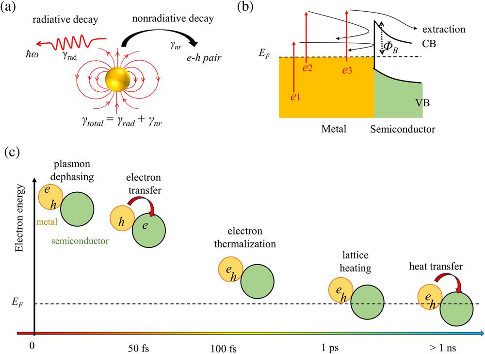

Set citation alerts for the article
Please enter your email address
© Copyright 2018-2021 | Chinese Laser Press. All Rights Reserved 沪ICP备15018463号-20