• Journal of Infrared and Millimeter Waves
  • Vol. 40, Issue 5, 595 (2021)
Guo-Shuai WEI1, Rui-Ting HAO1、*, Jie GUO1, Xiao-Le MA1, Xiao-Ming LI1, Yong LI1, Fa-Ran CHANG1, Yu ZHUANG1, Guo-Wei WANG2、3、**, Ying-Qiang XU2、3, Zhi-Chuan NIU2、3, and Yao WANG4
Author Affiliations
  • 1School of Energy and Environment Science,Yunnan Normal University,Kunming 650092,China
  • 2State Key Laboratory for SLs and Microstructures,Institute of Semiconductors,Chinese Academy of Sciences,Beijing 100083,China
  • 3Synergetic Innovation Center of Quantum Information and Quantum Physics,University of Science and Technology of China,Hefei 230026,China
  • 4National Center for International Research on Green Optoelectronics,Guangdong Provincial Key Laboratory of Optical Information Materials and Technology,Institute of Electronic Paper Displays,South China Academy of Advanced Optoelectronics,South China Normal University,Guangzhou 510006,China
  • show less
    DOI: 10.11972/j.issn.1001-9014.2021.05.005 Cite this Article
    Guo-Shuai WEI, Rui-Ting HAO, Jie GUO, Xiao-Le MA, Xiao-Ming LI, Yong LI, Fa-Ran CHANG, Yu ZHUANG, Guo-Wei WANG, Ying-Qiang XU, Zhi-Chuan NIU, Yao WANG. High quality strain-balanced InAs/InAsSb type-II superlattices grown by molecular beam epitaxy[J]. Journal of Infrared and Millimeter Waves, 2021, 40(5): 595 Copy Citation Text show less
    Schematic illustration of mechanical shutter sequences used in growing(a)InAs/GaSb and(b)InAs/InAsSb superlattices.
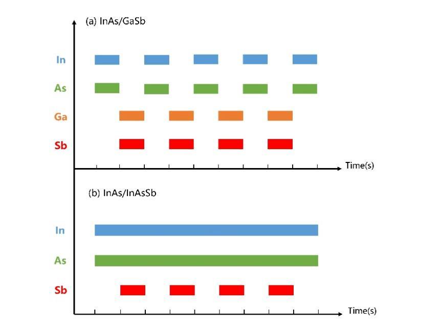
    Fig. 1. Schematic illustration of mechanical shutter sequences used in growing(a)InAs/GaSb and(b)InAs/InAsSb superlattices.
    The GaSb substrate surface reconstitution diffraction stripe varies with substrate temperature. (a) 2×5, (b) 1×3
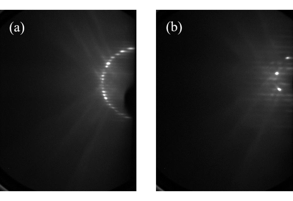
    Fig. 2. The GaSb substrate surface reconstitution diffraction stripe varies with substrate temperature. (a) 2×5, (b) 1×3
    The mechanical shutter sequence during growth(Contains InSb interface)
    Fig. 3. The mechanical shutter sequence during growth(Contains InSb interface)
    AFM image of spike-like defects in an area of 10µm×10µm:Tc+15°C Tc Tc-15°C Tc-25°C
    Fig. 4. AFM image of spike-like defects in an area of 10µm×10µm:Tc+15°C Tc Tc-15°C Tc-25°C
    Trend of the number of spike-like defects with temperature in a 10µm×10µm area
    Fig. 5. Trend of the number of spike-like defects with temperature in a 10µm×10µm area
    The high-resolution x-ray diffraction(HRXRD)of the three sets of InAs/InAsSb SLs samples with the BEP flux ratio. S1:Sb/In=3.1,S2:Sb/In=2,S3:Sb/In=1.
    Fig. 6. The high-resolution x-ray diffraction(HRXRD)of the three sets of InAs/InAsSb SLs samples with the BEP flux ratio. S1:Sb/In=3.1,S2:Sb/In=2,S3:Sb/In=1.
    (a) HRXRD of measurement (black) and simulations (red) of InAs/InAs0.66Sb0.34 SL.:(b)Structure used for HRXRD simulation before shutter sequence optimization
    Fig. 7. (a) HRXRD of measurement (black) and simulations (red) of InAs/InAs0.66Sb0.34 SL.:(b)Structure used for HRXRD simulation before shutter sequence optimization
    The images of the mechanical shutter sequence of each sources cell shutter.(Uninsert InSb interface)
    Fig. 8. The images of the mechanical shutter sequence of each sources cell shutter.(Uninsert InSb interface)
    (a) HRXRD of three sets of samples with different Sb/In: S1, Sb/In=1; S2, Sb/In=2; S3, Sb/In=3.1; (b) Variation of strain and xsb with Sb/In in InAs/InAs1-xSbx superlattices.
    Fig. 9. (a) HRXRD of three sets of samples with different Sb/In: S1, Sb/In=1; S2, Sb/In=2; S3, Sb/In=3.1; (b) Variation of strain and xsb with Sb/In in InAs/InAs1-xSbx superlattices.
    (a) HRXRD of S1 (black) and simulations (red) of InAs/InAs0.66Sb0.34 SL. The inset shows the separation between the GaSb substrate and SL 0th-order peak.:(b)Structure used for HRXRD simulation after shutter sequence optimization
    Fig. 10. (a) HRXRD of S1 (black) and simulations (red) of InAs/InAs0.66Sb0.34 SL. The inset shows the separation between the GaSb substrate and SL 0th-order peak.:(b)Structure used for HRXRD simulation after shutter sequence optimization
    AFM images of (a)Tc-15°C, (b)Tc, (c)Tc+15°C InAs/InAs0.66Sb0.34 SL samples surface morphology over 10µm×10µm.
    Fig. 11. AFM images of (a)Tc-15°C, (b)Tc, (c)Tc+15°C InAs/InAs0.66Sb0.34 SL samples surface morphology over 10µm×10µm.
    The variation trend of 0th-order peak FWHM values and surface RMS roughness at different growth temperatures.
    Fig. 12. The variation trend of 0th-order peak FWHM values and surface RMS roughness at different growth temperatures.
    The FTIR absorption spectrum of InAs/InAs0.66Sb0.34 superlattice.
    Fig. 13. The FTIR absorption spectrum of InAs/InAs0.66Sb0.34 superlattice.
    PL spectrum of the InAs/InAs0.66Sb0.34 SL at different temperatures.
    Fig. 14. PL spectrum of the InAs/InAs0.66Sb0.34 SL at different temperatures.
    Guo-Shuai WEI, Rui-Ting HAO, Jie GUO, Xiao-Le MA, Xiao-Ming LI, Yong LI, Fa-Ran CHANG, Yu ZHUANG, Guo-Wei WANG, Ying-Qiang XU, Zhi-Chuan NIU, Yao WANG. High quality strain-balanced InAs/InAsSb type-II superlattices grown by molecular beam epitaxy[J]. Journal of Infrared and Millimeter Waves, 2021, 40(5): 595
    Download Citation