1School of Energy and Environment Science,Yunnan Normal University,Kunming 650092,China
2State Key Laboratory for SLs and Microstructures,Institute of Semiconductors,Chinese Academy of Sciences,Beijing 100083,China
3Synergetic Innovation Center of Quantum Information and Quantum Physics,University of Science and Technology of China,Hefei 230026,China
4National Center for International Research on Green Optoelectronics,Guangdong Provincial Key Laboratory of Optical Information Materials and Technology,Institute of Electronic Paper Displays,South China Academy of Advanced Optoelectronics,South China Normal University,Guangzhou 510006,China
In this paper, high quality InAs/InAsSb(Ga-free) type-II superlattice were grown on GaSb substrates by molecular beam epitaxy. The superlattice layers structure consists of 100 periods with 3.8 nm thick InAs layers and 1.4 nm InAs0.66Sb0.34 layers. A specific spike-like defect was found during experiment. The epitaxial layer was characterized and analyzed by high-resolution x-ray diffraction (HRXRD), atomic force microscope (AFM) and Fourier transform infrared spectroscopy (FTIR). The results show that the optimized sample is almost zero lattice mismatched, the FWHM of the zeroth order SL peak is 39.3 arcsec, the RMS surface roughness achieves around 1.72? over an area of 10 μm×10 μm. The FTIR absorption spectrum shows a 50% cutoff wavelength of 4.28 μm. And PL spectrum shows that the peak of InAs/InAs0.66Sb0.34 SL is at 4.58 μm. These initial results indicate that the grown InAs/InAsSb SL is stable and reproducible, and thus it is worthy of further investigation.
After more than half a century of development,infrared detectors have made great progress by developing infrared detectors and focal planes based on a series of material systems such as HgCdTe,InSb,quantum well and Type-II superlattices(T2SLs). Type-II superlattices have been identified as one of the most promising types of alternative materials,[1-3] since the concept of the superlattice was introduced in the 1970s. Infrared detectors based on InAs/GaSb T2SLs have come a long way in the last few decades[4].In addition,the InAs/GaSb T2SLs could be grown by using different equipments and substrates to produce high performance materials and devices without traditional growth methods[5-7].However,the InAs/GaSb T2SLs still have their limitations due to the low minority carrier lifetime,resulting in performance that does not approach the theoretical limit. At present,the measured carrier lifetime of InAs/GaSb T2SLs is typically below 100 ns and is limited by the SRH mechanism. The origin of the above recombination centers has been attributed to the presence of gallium[8].Hence,Ga-free InAs/InAsSb superlattices emerged,aiming to fundamentally eliminate gallium-related intrinsic defects,thereby reducing the SRH recombination probability and increasing carrier lifetime[9].Currently,infrared detectors based on the InAs/InAsSb superlattice have been demonstrated excellent performance[10].
InAs/InAsSb and InAs/GaSb T2SLs have a lot in common:first of all,they both can achieve lattice matching with GaSb substrates(InAs/InAsSb requires adjustment of components);Then,they can cover most of the infrared spectrum;Besides,they both respond to the infrared signal by electron-absorbing photons from the top of the hole microstrip to the bottom of the electronic microstrip. Changing the composition and thickness of the superlattice can adjust the microstrip position and band gap width,thus achieving a similar effect of adjusting the band gap width of the bulk material.
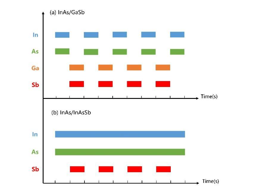
In general,InAs/InAsSb T2SLs are relatively simple to grow,and Fig. 1 briefly illustrates the growth shutter sequences of the two superlattices. Because of the absence of Ga in the SL layers,the interfacial control was found to be more straight-forward in these structures.[11] All we have to do is to control the Sb shutter switch. Of course,this does not include the growth of the interface,the actual growth process is a bit more complicated. And unlike InAs/GaSb T2SLs,InAs/InAsSb is not composed of lattice-matching materials,with InAs having a lattice constant of about 6.0583 and InSb having a lattice constant of about 6.4794,the resulting lattice mismatch leads to changes in superlattice structure and energy bands. Nonetheless,it has been found to accommodate up to 7% lattice mismatch without the formation of dislocations. The thickness of the strained epitaxial layers is limited by the critical thickness[12].
Figure 1.Schematic illustration of mechanical shutter sequences used in growing(a)InAs/GaSb and(b)InAs/InAsSb superlattices.
In order to better absorb photons,in the structural design,the periodic thickness of the superlattice needs to be as thin as possible. The increase in Sb components causes the superlattice to produce a compressive strain,requiring more InAs to produce tensile strain to compensate,which in turn causes the InAs layer to thicken,resulting in a thickening of the overall period thickness. Therefore,these parameters should be taken into account when designing the structure to achieve the desired result. In this paper,we use molecular beam epitaxy(MBE)to grow InAs/InAsSb strain-balanced type-II superlattices directly on GaSb substrates,which provides an idea condition for the stable and repeatable growth of InAs/InAsSb T2SLs and lays a solid foundation for the follow-up device research.
1 Experimental
MBE(molecular beam epitaxy)is a powerful technique for epitaxial growth with excellent crystalline quality,good compositional and doping uniformity. Given the ability to precisely actuate the shutter sequences,MBE has been successfully applied for superlattice growth where the layer thickness needs to be under perfect control. The doping levels can also be controlled with high precision[13]. The epitaxial growth of all samples were grown in Veeco Gen II MBE system on a n-type GaSb(001)substrate,which was equipped with valved cracker sources for group V(Sb2 and As2)fluxes and Ga/In cells. MBE control software is used to simultaneously control the temperature ramps,shutter operation,and As and Sb cracking-cell valve positions[14]. Before each growth of functional layer,the oxide on the surface of the GaSb substrate was removed by deoxidizing at 630°C for 30 minutes,and then the surface was flattened by growing a GaSb buffer at 550°C for a certain time(the normal growth time is 30min,about 260~300 nm). As far as the facility in the experiment is concerned,when the Sb beam is 9.26×10⁻⁷ Torr(1Torr = 1.33322×10² Pa),in-situ reflection high-energy electron diffraction(RHEED)was used to monitor the temperature at which the substrate surface transitions from 2×5 to 1×3(shown in Fig. 2),this transition occurred at a substrate temperature of [15]. is defined as the crossover temperature at which a GaSb surface reconstruction(2×5↔1×3)at a given antimony stabilization flux.
Ga-free / T2SLs can be strain-balanced on GaSb by adjusting the appropriate combinations of layer thicknesses and alloy compositions. Typically,the tensile strain in InAs is compensated by the compressive strain introduced in leading to a thicker InAs layer compared to the InAsSb one(for antimony concentration > 0.18).[16] Therefore,strain balancing is achieved theoretically by setting the average lattice parameter of one period of the SL equal to the lattice parameter of GaSb. In this work,the SL layers structure consists of 100 periods with 3.8 nm thick InAs layers and 1.4 nm layers. Before that,the growth was carried out firstly by a 274 nm thick GaSb buffer layer deposited on GaSb(001)substrates. In the whole process,the indium speed was kept constant at 0.4ML/s.
For all the samples,surface morphology was characterized by digital S–II Nano Navi atomic force microscope(AFM)in tapping mode at room temperature in air. The JV-QC3 HRXRD was employed to identify the strain,composition and growth quality of superlattice. The optical properties was measured by Thermo Scientific Nicolet iS-50 Fourier transform infrared spectroscopy(FTIR).
2 Ga-free SL growth details
2.1 strain-balance and component control
If the InAs/InAs1-xSbx superlattice is regarded as an InAsSb bulk material,it can be calculated that the Sb component in InAs1-xSbx occupies 9% of the total amount of group V elements when matching to a GaSb substrate. However,the Sb component in the InAs1-xSbx layer we designed accounts for 34% and contains more InSb bonds,so it is not appropriate to use high substrate temperature for the InAs/InAs1-xSbx superlattice. And the V/III beam equivalent pressure(BEP)flux ratio was set to about 6 for As:In,3.1 for Sb:In,based on the theoretical composition. The mechanical shutter sequence during growth is shown in Fig. 3. A 6-second interruption and a 0.5-second InSb interface are added before and after the growth of the InAs layer(30s)and InAs1-xSbx layer(10s). The InSb interface has a certain effect on blocking the replacement of group Ⅴ elements. However,the morphology of the material grown in this way has many spike-like defects,which is interesting that they are not as dense as quantum dots but much higher than quantum dots,as shown in Fig. 4. The density of these spikes decreased with the decreasing temperature,and combined with the results shown in Fig. 4 and Fig. 5,it should be noticed that the temperature decrease from Tc+15°C to Tc-25°C reduced the number of spike-like defects from 30 to 13 in an area of 10µm×10µm. This implied that the stress in the InAs/InAsSb superlattice has a significant effect on the penetrating dislocations in the material,and the decrease of temperature does contribute to the reduction of defect density.[17] However,since the lattice mismatch was still too large at this point,it didn’t eliminate the spike-like defects.
Figure 3.The mechanical shutter sequence during growth(Contains InSb interface)
Several experiments were carried out to change the Sb:In BEP flux ratio while keeping the As:In BEP flux ratio unchanged. Three sets of InAs/InAsSb SLs(S1,S2,S3)with the same As:In BEP flux ratio of 6 but different Sb:In BEP flux ratio of 3.1,2,and 1 were grown,respectively. The lattice matching of the samples was analyzed by the HRXRD and the results are shown in Fig. 6.
Figure 6.The high-resolution x-ray diffraction(HRXRD)of the three sets of InAs/InAsSb SLs samples with the BEP flux ratio. S1:Sb/In=3.1,S2:Sb/In=2,S3:Sb/In=1.
It can be clearly seen from the above XRD diffraction pattern that the strain is getting closer to the GaSb substrate peak as the Sb:In BEP flux ratio is reduced. The strain between the GaSb substrate peak and the InAs/InAsSb SL zero order peak are(S1)-494 arcsec,(S2)-305 arcsec,(S3)-207 arcsec,respectively. However,even the Sb:In BEP flux ratio is reduced to 1,it still shows compressive strain,indicating that antimony component is greater than 9% in total InAs/InAs1-xSbx SL. There are two reasons resulting in this situation:① The concentration of the group V element required to grow the best GaSb buffer layer is too high,while the group V concentration required to grow the InAs1-xSbx layer is relatively low. So that the strain of the superlattice is difficult to control;② Due to the accuracy of the device,the shutter time of 0.5s cannot be accurately controlled,which also caused the background density of antimony to increase. In order to solve the problem of excessive Sb content,the growth process was optimized. We simulated the HRXRD pattern containing the InSb interfacial structure and compared it with the measurement of S3,as shown in Fig 7(a). The structure used for HRXRD simulation is shown in Fig 7(b). The simulated results show that the separation between the SL zero order peak and the substrate peak is wide,which is consistent with the experimental results. This indicates that it is difficult to balance the stresses by adding the InSb interface with the defined period thickness and constituents. So we consider it would be helpful to remove the 0.5s InSb interface included during growth process. The mechanical shutter sequence during growth is shown in Fig. 8.
Figure 7.(a) HRXRD of measurement (black) and simulations (red) of InAs/InAs0.66Sb0.34 SL.:(b)Structure used for HRXRD simulation before shutter sequence optimization
By removing the 0.5s InSb shutter before and after growing the InAsSb layer,the Sb content was effectively controlled. We still grew three sets of samples(S4,S5,S6)with Sb:In:3.1,2,and 1,respectively,and the XRD images are shown in Fig. 9(a),which shows that the strain decreases to almost zero after Sb:In decreases from 3.1 to 1.The lattice matched InAs/InAs1-xSbx SL was acquired. We analyze that the change of shutter order makes the mismatch decrease,mainly because it changes the interface component and reduces the Sb content,which makes the mismatch decrease,but the lattice constant of InSb is larger,so the removal of InSb interface also reduces the period thickness to some extent. The final experimental results prove that using the growth interruption method shown in Figure 8 for InAs/InAsSb epitaxy will be easier to control the components and the surface quality will be better.
Figure 9.(a) HRXRD of three sets of samples with different Sb/In: S1, Sb/In=1; S2, Sb/In=2; S3, Sb/In=3.1; (b) Variation of strain and xsb with Sb/In in InAs/InAs1-xSbx superlattices.
Through the spectral analysis of XRD,the periodic thickness of the superlattice can be calculated by the distance between the adjacent satellite peaks produced by symmetrical diffraction,as shown in Eq.(1):
,
where D is the periodic thickness, is the wavelength of incident X-ray beam(=1.5406Å), is the separation distance between two adjacent satellite peaks and (30.3634°)is the Bragg angle of the GaSb substrate. was took as the distance between the +1 order peak(the abscissa is 3615 arcsec)and the +2 order peak(the abscissa is 7225 arcsec),and the calculated period thickness of S1 is 51.01Å,which is within the allowable error range of the expected design period thickness.
When the material grows on the substrate,within the elastic range,the lattice grows coherently,which for an atom means that it is stretched or compressed along the growth direction(assumed to be the Z direction),and its vertical strain satisfies Eq.(2). In the process of heteroepitaxial epitaxy,an equation for the strain of the epitaxial film and the substrate is defined as Eq.(3).
where and represent the lattice growth direction(vertical direction), and is the lattice constant of the epitaxial film and substrate,respectively. is the Poisson ratio of the epitaxial film. Δ = - is the distance between the diffraction peak of the epitaxial film and the substrate peak, is the position of the main peak of the superlattice(0th-order peak).
Epitaxial layers are generally considered lattice matched when the peak separation is below 100 arcseconds,or 0.0825% for GaSb substrates.[18] The Sb mole fraction()of the InAs/InAs1-xSbx superlattices is obtained by extracting the information from Fig. 9(a)and calculating it,as shown in Fig. 9(b),which shows that the Sb constituents decreases with the decrease of Sb:In,and is 0.331 at Sb/In=1,which meets our design expectation. We have performed XRD simulations of the pre-designed superlattice structure,period and components and obtained a better fit,as shown by the red line in the lower half of Fig. 10(a). The structure used for HRXRD simulation after shutter sequence optimization is shown in Fig. 10(b). Comparing the HRXRD image of S4(black lines in the upper half)with the simulation results,we can see that they have a very high agreement,so we can conclude that the components are very accurately controlled in the actual epitaxial growth process. In Fig. 10,the separation between the InAs/InAsSb SL 0th-order peak and the substrate is only 44 arcsec,corresponding to an in-plane lattice mismatch of ~0.04%,almost reaching the zero lattice mismatch. At the same time,those special spike-like defects disappeared,which further proved that it was caused by excessive stress. HRXRD spectrum shows the satellite peaks of superlattice were sharp and intense. The value of full-width at half-maximum(FWHM)can reflect the growth quality of the material to some extent and the FWHM of the first order SL peak is 42 arcsec in HRXRD pattern. The Sb mole fraction()calculated by the above formula is 0.331,which is consistent with the pre-designed structural composition. This indicates that the superlattice has better strain balance and higher growth quality when the Sb composition in the InAs/InAs1-xSbx layer is close to 35% at the designed periodic thickness,which confirmed with each other in the conclusion of Hua Li and Yong-Hang Zhang 's paper.[17]
Figure 10.(a) HRXRD of S1 (black) and simulations (red) of InAs/InAs0.66Sb0.34 SL. The inset shows the separation between the GaSb substrate and SL 0th-order peak.:(b)Structure used for HRXRD simulation after shutter sequence optimization
During the growth of InAs/InAs1-xSbx T2SL,substrate temperature has a great influence on the structural quality and optical properties.[19] At the same time,it should also be considered that the growth of mixed anion alloys is complicated by the potential reaction of As2 with Sb surfaces.[20] Therefore,it is very important to find the most suitable substrate temperature. For III-group atoms,lower growth temperature makes better adhesion,but high growth temperature makes it difficult to adhere resulting in the formation of some holes on the surface;For V-group atoms,when the growth temperature is high,it would be beneficial for the desorption of excess V-group atoms,providing the better migration environment for surface atoms. On the contrary,the low growth temperature would cause insufficient diffusion of the V-group atoms,resulting in the shape of the river gully and the surface atomic steps are not formed. According to the optimized parameters and the above theoretical support,three sets of InAs/InAsSb SL samples with different deposition temperature were grown at Tg = Tc-15°C,Tg = Tc,Tg = Tc+15°C. Then,their 10×10 µm AFM images are shown in Fig. 11.
Figure 11.AFM images of (a)Tc-15°C, (b)Tc, (c)Tc+15°C InAs/InAs0.66Sb0.34 SL samples surface morphology over 10µm×10µm.
Through AFM analysis,the evolution of the surface morphology was studied. It can be seen from Fig. 11(a)that when the growth temperature is Tc -15°C,the superlattice surface is grooved and no atomic steps appear,indicating that although the surface III-group atoms have a good adhesion,but the V-group atoms are not sufficiently diffused,inferring the higher growth temperature should be applied at this stage. As can be seen from Fig. 11(c),when the growth temperature is Tc+15°C,the surface is relatively flat,but there are several holes,which are caused by the lack of III-group atoms. This indicates that the V-group atoms on the surface of the material have been fully desorbed and migrated,while the III-group atoms are not fully adhered,so it is inferred that the growth temperature at Tc+15°C is slightly higher. Fig. 11(b)shows the morphology at a growth temperature of Tc. The atomic step on the surface is clearly observed,the undulating condition of the surface was also the lowest among these three samples,indicating that this temperature is the most appropriate.
Fig. 12 show the variation trend of 0th-order peak FWHM values and surface RMS roughness at different growth temperatures. It can be seen that the trend of FWHM and RMS roughness is consistent,with both the FWHM and RMS roughness of the material being the smallest at Tc,only 39.3 arcsec and 1.72 Å,respectively. When the temperature is Tc+15°C and Tc-15°C,i.e. the temperature increases or decreases,the values of both FWHM and RMS roughness increase,which also proves the superior crystalline quality and a high reproducibility rate at the growth temperature of Tc.
Figure 12.The variation trend of 0th-order peak FWHM values and surface RMS roughness at different growth temperatures.
In terms of optical properties,the FTIR absorption spectrum and photoluminescence spectra were used to determine the cutoff wavelength or band gap of the sample. Fig. 13 shows the 50% cut-off wavelength is 4.28 µm and it is completely cut off at 5.1 µm at 300 K. Note that there is a steep absorption band at 4.3 µm,indicating that there is significant absorption here. The steepness of the absorption band edge is related to the intermixing and roughness of the interface atoms. The entire absorption edge is relatively smooth,indicating that the structure of the superlattice is complete and the interface is in good condition. It also exhibits a series of characteristics associated with transitions between the lowest conduction band and the various valence sub-bands,[21] and there is no other transitions between energy bands caused by defect energy levels. As shown in Fig. 14,the PL spectrum of the InAs/InAs0.66Sb0.34 SL were conducted at different temperatures. The excitation source uses a semiconductor pumped solid-state laser with a power of 150 mW and a laser wavelength of 405 nm,and the laser power is adjusted by an attenuator. It can be seen that the noise of the spectral peak at T=100 K is relatively large. When the temperature decreases to 50 K and 4 K,a clear luminescence peak appears. The wavelength corresponding to the spectral peak showed a weak blue shift with the decrease of temperature,which is more common in narrow bandgap semiconductors. When T=4 K,the luminescence peak is the clearest and sharpest,indicating that the material possesses excellent optical properties. The wavelength of the peak is at 4.58 μm,which is in the mid-wave band and meets the design expectation.
Figure 13.The FTIR absorption spectrum of InAs/InAs0.66Sb0.34 superlattice.
In summary,we have investigated the growth conditions and optical properties of InAs/InAs0.66Sb0.34 type-II superlattice on GaSb substrates by molecular beam epitaxy. Experimental results demonstrate that a suitable and stable V/III BEP flux ratio and substrate temperature are essential for obtaining reproducibly grown InAs/InAsSb superlattices. When V/III BEP flux ratio was As:In=6 and Sb:In=1,with optimized proper growth procedures,the separation between the InAs/InAsSb SL 0 th-order peak and the substrate is only 44 arcsec,almost reaching zero lattice mismatch. The FWHM of the first order SL peak is 42 arcsec in HRXRD pattern. When the optimized growth temperature is Tc,the FWHM of the zeroth order SL peak is 39.3 arcsec,the RMS surface roughness achieves around 1.72Å over an area of 10µm×10 µm. The FTIR absorption spectrum shows the 50% cut-off wavelength is 4.28 µm and the whole absorption edge is relatively smooth. And PL spectrum shows that the peak of InAs/InAs0.66Sb0.34 SL is at 4.58 μm. The above results show that the high-quality strain-balanced InAs/InAsSb type II superlattice was prepared. Therefore,our experimental process and results may be useful for further experimental and theoretical studies on infrared detectors based on InAs/InAsSb superlattice.