• Chinese Optics Letters
  • Vol. 20, Issue 1, 011302 (2022)
Junbo Zhu1、2, Haiyang Huang1, Yingxuan Zhao1, Yang Li1、2, Zhen Sheng1、*, and Fuwan Gan1、3、**
Author Affiliations
  • 1State Key Laboratory of Functional Materials for Informatics, Shanghai Institute of Microsystem and Information Technology, Chinese Academy of Sciences, Shanghai 200050, China
  • 2University of Chinese Academy of Sciences, Beijing 100049, China
  • 3School of Future Technology, University of Chinese Academy of Sciences, Beijing 100049, China
  • show less
    DOI: 10.3788/COL202220.011302 Cite this Article Set citation alerts
    Junbo Zhu, Haiyang Huang, Yingxuan Zhao, Yang Li, Zhen Sheng, Fuwan Gan. Efficient silicon integrated four-mode edge coupler for few-mode fiber coupling[J]. Chinese Optics Letters, 2022, 20(1): 011302 Copy Citation Text show less

    Abstract

    Here, we designed a broadband, low loss, compact, and fabrication-tolerant silicon-based four-mode edge coupler, composed of a 1×3 adiabatic mode-evolution counter-taper splitter and a triple-tip inverse taper. Based on mode conversion and power splitting, the proposed structure can simultaneously realize efficient mode coupling from TE0, TM0, TE1, and TM1 modes of multimode silicon waveguides to linearly polarized (LP), LP01,x, LP01,y, LP11a,x, and LP11a,y, modes in the few-mode fiber. To the best of our knowledge, we proposed the first scheme of four LP modes coupling, which is fully compatible with standard fabrication process. The 3D finite-difference time-domain simulation results show that the on-chip conversion losses of the four modes remain lower than 0.62 dB over the 200 nm wavelength range, and total coupling losses are 4.1 dB, 5.1 dB, 2.1 dB, and 2.9 dB for TE0-to-LP01,x, TM0-to-LP01,y, TE1-to-LP11a,x, and TM1-to-LP11a,y, respectively. Good fabrication tolerance and relaxed critical dimensions make the four-mode edge coupler compatible with standard fabrication process of commercial silicon photonic foundries.

    1. Introduction

    Silicon photonics has been attracting lots of attention in recent years[1], benefiting from the compatibility with standard complementary metal-oxide-semiconductor (CMOS) fabrication technology, which significantly reduces the fabrication cost of silicon photonic devices. The silicon-on-insulator (SOI) platform has been widely used in on-chip communication systems with low insertion loss and small footprint[2,3]. Meanwhile, in order to satisfy the rapidly increasing demands on high capacity and low power consumption data transfer, mode-division multiplexing (MDM) has also emerged as an efficient approach to further increase the transmission capability[4] with the introduction of high-order modes in both fibers and silicon chips[5,6]. Many on-chip multichannel mode (de)multiplexers have been developed[79], but, in order to implement a complete on-chip MDM optical network, large data transmission capacity and low-loss coupling between few-mode fibers (FMFs) and on-chip multimode waveguide are also highly needed[10].

    It is a challenging task to design efficient couplers with large bandwidths, low insertion loss, and small footprint that connect on-chip multimode waveguides and FMFs due to their huge mode mismatch. Vertical and edge coupling schemes are the most common ways to realize multimode fiber-chip coupling. For vertical coupling, grating couplers (GCs)[1114] are usually used due to their small footprint and large misalignment tolerance. However, the GCs are intrinsically sensitive to fabrication error and wavelength, which significantly limit their application in broadband wavelength-division multiplexing (WDM). Compared with GCs, edge couplers can overcome the drawbacks of polarization/wavelength sensitivity. The 3D-mode multiplexer structure based on multilayer asymmetric waveguide branches has been reported for four-mode coupling[15], while the fabrication becomes complicated for different waveguide heights. Multi-stage silicon inverse taper couplers with polymer up-cladding realized four linearly polarized (LP) modes coupling[16], but the large total length (2.68 mm) and lack of compatibility with standard CMOS fabrication process limited its application. The double-tip inverse taper was demonstrated to realize the first, to the best of our knowledge, high-order mode coupling[17], and some three inverse tapers for two-mode coupling have been reported[10,18] with large mode conversion losses and coupling losses[10]. Although these types of couplers mentioned can meet some performance requirements, it is a challenge for an on-chip multimode coupler to simultaneously satisfy compact, low loss, wavelength-independent, and CMOS compatibility.

    In this Letter, we report a silicon edge coupler based on adiabatic taper for four-mode fiber-to-chip coupling. The proposed coupler consists of a 1×3 adiabatic mode-evolution counter-taper splitter and a triple-tip inverse taper. The 3D finite-difference time-domain (FDTD) simulation results show that the on-chip conversion losses of the four-mode edge coupler (FMEC) are 0.01 dB, 0.02 dB, 0.07 dB, and 0.27 dB for the input TE0, TM0, TE1, and TM1 modes at 1.55 µm wavelength, respectively, and, in the wavelength range from 1.45 to 1.65 µm, the mode conversion loss remains lower than 0.62 dB. Meanwhile, the designed feature size is 100 nm, which is compatible with the standard process of commercial silicon photonic foundries. The calculated total coupling losses between the edge coupler and FWF are 4.1 dB, 5.1 dB, 2.1 dB, and 2.9 dB for TE0-to-LP01,x, TM0-to-LP01,y, TE1-to-LP11a,x, and TM1-to-LP11a,y, respectively. Moreover, the fabrication tolerance analysis confirms that the FMEC remains fairly low loss within a large deviation range (±50nm for silicon waveguide width).

    2. Operation Principle and Device Design

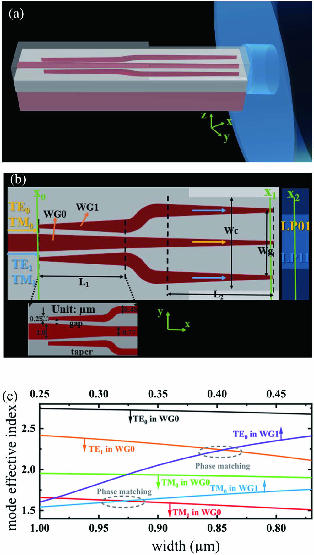
    Figure 1(a) presents the schematic of the designed FMEC, which consists of a 1×3 adiabatic mode-evolution counter-taper splitter and a triple-tip inverse taper. The FMEC is designed on an SOI wafer with 220 nm thick top silicon layer, 4.5 µm thick upper SiO2 cladding, and 3 µm thick bottom SiO2 cladding. The operation principle in the FMEC is based on the mode evolution in a coupler that has two waveguides with cores counter-tapered[19,20]. As shown in Fig. 1(b), the width of the upper waveguide (WG1) increases from 0.25 to 0.48 µm, whereas the width of the bottom waveguide (WG0) varies from 1.0 µm to 0.77 µm. We use Lumerical finite-difference eigenmode (FDE) solver to calculate the effective refractive indices of TE0, TM0, TE1, and TM1 in WG0 and those of TE0 and TM0 in WG1 at the 1.55 µm wavelength. As we can see, there is a cross point for TE1 in WG0 and TE0 in WG1, TM1 in WG0 and TM0 in WG1, respectively, which means the input TE1 and TM1 modes in WG0 can adiabatically convert to the TE0 and TM0 modes in the adjacent WG1, respectively. There is no cross point with their own polarization modes for the TE0 and TM0 curves of WG0, which means the input TE0 and TM0 modes will remain propagating in the central waveguide. The width difference for both sides of tapers is chosen as 0.23 µm to ensure a large difference of effective indices, where the converted mode would not be coupled back. Thus, in the FMEC, the input TE0 and TM0 modes will be mapped to the central output. The input TE1 and TM1 modes can be converted and divided into two TE0 modes and two TM0 modes with identical intensity and out-phase, and eventually output through the upper and bottom single-mode waveguides of the FMEC separately. For the triple-tip inverse taper, as the waveguide narrows, the middle inverse taper converts the mode field (TE0/TM0 mode) confined in the silicon waveguide into the clad layer, collected by the FMF, and eventually evolves into LP01,x and LP01,y modes. The mode fields of two side inverse tapers keep expanding between the taper tips and convert into the TE1/TM1 mode field at the edge of the chip, collected by FMF, and eventually evolve into the LP11,x and LP11,y modes.

    Schematics of DMEC coupling with dual-mode fiber in (a) 3D view and (b) top view; the silicon waveguides are in red, and the silicon oxide layer is in gray. The modes conversion process is also demonstrated. (c) Effective refractive index of the modes in each waveguide (WG0/WG1) of the mode-evolution counter-taper with tapering width from 1 µm/0.25 µm to 0.77 µm/0.48 µm.

    Figure 1.Schematics of DMEC coupling with dual-mode fiber in (a) 3D view and (b) top view; the silicon waveguides are in red, and the silicon oxide layer is in gray. The modes conversion process is also demonstrated. (c) Effective refractive index of the modes in each waveguide (WG0/WG1) of the mode-evolution counter-taper with tapering width from 1 µm/0.25 µm to 0.77 µm/0.48 µm.

    3. Simulation and Analysis

    3.1. Optimization of FMEC

    To analyze the performance of FMEC, the simulation is separated into two parts, the on-chip mode conversion from x0x1 in Fig. 1(b), and the spatial mode coupling from the triple-tip inverse taper to the fiber [x1x2 in Fig. 1(b)]. First, we use the eigenmode expansion (EME) solver to optimize the taper length (L1, L2), and the parameters used in simulation are shown in Fig. 1(b). In order to satisfy the feature size of commercial silicon foundries, the gaps between the upper and bottom tapers are all set to be 200 nm, and the taper tip width is set to be 100 nm. Figures 2(a) and 2(b) show the losses from the 1×3 adiabatic mode-evolution counter-taper splitter (L1) and inverse taper (L2) at the 1.55 µm wavelength. The mode conversion losses are less than 0.2 dB when L1>230µm, and propagation losses in the inverse taper are less than 0.6 dB when L2>400µm. Here, we choose L1=250µm and L2=450µm to ensure a good trade-off between low loss and small footprint for both modes, and the length of the bending section between the 1 × 3 adiabatic mode-evolution counter-taper splitter and inverse taper is 40 µm, so the whole device has 740 µm total length. The on-chip conversion losses of FMEC are less than 0.01 dB, 0.02 dB, 0.07 dB, and 0.27 dB for the input TE0, TM0, TE1, and TM1 modes at the 1.55 µm wavelength, respectively, and, in the wavelength range from 1.45 to 1.65 µm, the mode conversion loss remains lower than 0.62 dB. With the optimized taper length, the transmission spectra of the designed mode-evolution part [x0x1 in Fig. 1(b)] are simulated via the 3D-FDTD solver, as shown in Fig. 2(c).

    (a) Mode conversion loss for the input TE0, TM0, TE1, and TM1 modes, respectively, (b) transmission loss for the TE0 and TM0 modes in inverse taper (L2), and (c) wavelength dependence of the transmission from ‘x0’–‘x1’.

    Figure 2.(a) Mode conversion loss for the input TE0, TM0, TE1, and TM1 modes, respectively, (b) transmission loss for the TE0 and TM0 modes in inverse taper (L2), and (c) wavelength dependence of the transmission from ‘x0’–‘x1’.

    However, the coupling between the triple-tip taper and FMF presents larger coupling loss, mainly caused by the mismatched mode fields between chip edge and FWF. In the simulation model, the diameters of core and cladding of the FMF are 14 µm and 125 µm, with the refractive indices of 1.4485 and 1.44402, respectively. The silicon substrate may cause more loss because of leaky modes, so we remove the substrate of the SOI wafer[21,22], as shown in Fig. 3. In order to optimize the coupling loss, there are two parts we needed to analyze separately: the integral of mode overlap of the FMF and SiO2 cladding and the mode coupling loss between the FMF and silicon triple-tip taper. We first optimize the overlap integral in Fig. 4(a). The cladding width (Wc) [Fig. 1(b)] is chosen to be 19 µm in order to achieve largest average overlap for four modes. In the second step, we optimize the coupling loss of the silicon triple-tip taper with FMF, which is decided by the taper tip width and the gap spacing (Wg) between upper and bottom tapers for TE1 and TM1 modes. Figure 4(b) shows the coupling losses for different Wg. The Wg is chosen to be 9 µm. With the optimized parameters, we calculated the coupling losses between the triple-tip taper and FMF in 3D-FDTD, which are 4.0 dB, 5.0 dB, 2.0 dB, and 2.6 dB for TE0-to-LP01,x, TM0-to-LP01,y, TE1-to-LP11a,x, and TM1-to-LP11a,y, respectively, as shown in Fig. 4(c) (x1x2). Considering that those calculation results are based on the case of center excitation, we also simulate the lateral alignment tolerances of spatial mode coupling between the chip edge and FMF. In Fig. 4(d), the simulation results show that the coupling losses of LP01,x, LP01,y, LP11a,x, and LP11a,y present the 1 dB lateral alignment tolerances of 3 µm, 3.2 µm, 1.3 µm, and 1.3 µm. Therefore, we need a high accuracy alignment stage to measure the FMEC with high efficiency. Table 1 shows a comparison of the reported state-of-the-art multimode edge coupler. Compared to those types, the proposed FMEC exhibited low loss, more modes, and compatibility with CMOS.

    Ref.Number of ModesCompatible with CMOSCoupling Loss (dB)Evaluation Method
    [10]2YesTE0LP01:10.11Numerical
    2020TE1LP11:8.8
    [15]4NoLP01:8.8Experimental
    2017LP11a:9.0
    LP11b:9.6
    LP21a:9.9
    [17]1YesTE1LP11:3Numerical
    2017TE1LP11:5.5Experimental
    [16]4NoNo data/
    2020
    This work4YesTE0LP01,x:4.1Numerical
    TM0LP01,y:5.1
    TE1LP11a,x:2.1
    TM1LP11a,y:2.9

    Table 1. Comparison of the Reported Multimode Edge Coupler and Coupler Proposed in This Work

    Cross-sectional schematics of the edge coupling area: (a) x–y direction; (b) y–z direction.

    Figure 3.Cross-sectional schematics of the edge coupling area: (a) x–y direction; (b) y–z direction.

    (a) Simulated overlap integral of mode field between the FMF and SiO2 cladding, (b) simulated coupling loss for different Wg, (c) spatial mode coupling (from ‘x1’–‘x2’), and (d) the lateral alignment tolerance of coupling efficiency (CE) for spatial mode coupling.

    Figure 4.(a) Simulated overlap integral of mode field between the FMF and SiO2 cladding, (b) simulated coupling loss for different Wg, (c) spatial mode coupling (from ‘x1’–‘x2’), and (d) the lateral alignment tolerance of coupling efficiency (CE) for spatial mode coupling.

    The total coupling efficiency (CE) of the FMEC is 4.1 dB, 5.1 dB, 2.1 dB, and 2.9 dB for TE0-to-LP01,x, TM0-to-LP01,y, TE1-to-LP11a,x, and TM1-to-LP11a,y, respectively, and the crosstalk is less than 25dB with broadband operation, as the spectra of CE and crosstalk shown in Figs. 5(a) and 5(b). As a double-tip inverse taper coupling scheme has been proven for the first high-order mode coupling experimentally[17], we have good potential to realize efficient FMEC with fewer losses experimentally.

    (a) Total CE and (b) crosstalk of the FMEC in the span of 200 nm.

    Figure 5.(a) Total CE and (b) crosstalk of the FMEC in the span of 200 nm.

    Figures 6(a)6(p) show the simulated mode propagation for the input TE0, TM0, TE1, and TM1 modes, respectively, illustrating the mode conversion and coupling as we expected. Compared to the latest research[10], their simulation results show that the on-chip conversion efficiencies of the dual-mode edge coupler (DMEC) are 69% and 62% for TE0 and TE1, respectively, with 3 dB bandwidth of more than 200 nm. By using a multimode interference (MMI) structure, the large conversion loss enlarged the total coupling loss between the on-chip multimode waveguide and FWF, resulting in the total coupling loss of DMEC being more than 10 dB numerically. With our scheme, it can significantly reduce the on-chip conversion loss and scale up to four-mode coupling simultaneously.

    Simulated electrical field mode profiles of (a) TE0, (b) TM0, (c) TE1, and (d) TM1 modes at position ‘x0’ in Fig. 1(b); transmission profiles of the input (e) TE0, (f) TM0, (g) TE1, and (h) TM1 modes; mode profiles of the (i) TE0, (j) TM0, (k) TE1, and (l) TM1 modes in the SiO2 waveguide; mode profiles of (m) LP01,x, (n) LP01,y, (o) LP11a,x, and (p) LP11a,y modes supported in FMF.

    Figure 6.Simulated electrical field mode profiles of (a) TE0, (b) TM0, (c) TE1, and (d) TM1 modes at position ‘x0’ in Fig. 1(b); transmission profiles of the input (e) TE0, (f) TM0, (g) TE1, and (h) TM1 modes; mode profiles of the (i) TE0, (j) TM0, (k) TE1, and (l) TM1 modes in the SiO2 waveguide; mode profiles of (m) LP01,x, (n) LP01,y, (o) LP11a,x, and (p) LP11a,y modes supported in FMF.

    3.2. Analysis of fabrication tolerance

    In order to ensure reliability, Figs. 7(a) and 7(b) show the fabrication tolerance for on-chip conversion using EME by scanning the thickness and tapers waveguide width (which also causes gap distance variations), where the widths of both ends of the tapers vary simultaneously. Compared with that of high-order modes, the loss of input fundamental modes is negligible, so we only consider the conversion loss variations of the input TE1 and TM1 modes under the different fabrication error. The calculated conversion losses are always below 0.42 dB, as long as the waveguide width and thickness are controlled within the fabrication error variations of ±50nm and ±20nm, respectively, which can be readily achieved by commercial silicon photonics foundries. The fabrication tolerance of the mode conversion based on counter-tapers[23] and power splitting based on adiabatical tapers[24,25] have been proved. In addition, the tolerance simulation for the tip width was also performed. Considering 10% fabrication error, the increase of coupling loss between the inverse taper tip and fiber is below 0.28 dB, as shown in Fig. 7(c).

    Fabrication tolerance to deviation (a) of the waveguide width and thickness for TE1 input mode, (b) of the waveguide width and thickness for TM1 input mode, (c) of the tip width.

    Figure 7.Fabrication tolerance to deviation (a) of the waveguide width and thickness for TE1 input mode, (b) of the waveguide width and thickness for TM1 input mode, (c) of the tip width.

    4. Conclusions

    We design a compact, low loss, broadband, and fabrication-tolerant silicon photonic FMEC based on mode-evolution counter-tapers and a triple-tip inverse taper, serving as a bridge between the FMF and multimode chip, so that the input TE0, TM0, TE1, and TM1 modes can simultaneously couple into the FMF. The rigorous 3D-FDTD simulations show that the on-chip conversion losses of FMEC are 0.01 dB, 0.02 dB, 0.04 dB, and 0.27 dB for TE0, TM0, TE1, and TM1, respectively, and less than 0.62 dB in the wavelength range from 1.45 to 1.65 µm, which is negligible for the total coupling loss between FMEC and FMF compared with the coupling loss between triple-tip inverse taper and FMF. The total coupling losses are 4.1 dB, 5.1 dB, 2.1 dB, and 2.9 dB for TE0-to-LP01,x, TM0-to-LP01,y, TE1-to-LP11a,x, and TM1-to-LP11a,y, respectively, and less than 7 dB in the wavelength range from 1.45 to 1.65 µm theoretically. Considering fabrication and misalignment errors experimentally[17], we have the potential to realize efficient FMEC with fewer losses experimentally. The device’s compatibility with existing silicon photonics foundries and good fabrication tolerance enables the wide usage of the multimode edge coupler on a variety of silicon photonics applications. Considering the conversion loss is small enough for FMEC, further improvements could be adopted by reducing the coupling loss between the triple-tip inverse taper and FMF. A lensed or tapered FWF can be adopted to decrease the mode field area, which can obtain a better agreement with mode field distribution of FMEC. The inverse taper can also realize a better match of the mode field with the FMF and a larger misalignment tolerance through well-designed structures[2628]. Without a complex design and fabrication process, the proposed structure provides much more convenience for both designers and manufacturers. Meanwhile, it also shows good performance under the consideration of fabrication errors. Limited by the silicon thickness of SOI waveguides, this design cannot be applied to vertical higher-order modes, but, combining with different waveguided-core heights, it is also possible to develop more higher-order modes. Further improvements can be done to realize a better performance multimode edge coupler, which can be potentially used to further increase the transmission capability for optical interconnections and communications.

    References

    [1] C. Sun, M. T. Wade, Y. Lee, J. S. Orcutt, L. Alloatti, M. S. Georgas, A. S. Waterman, J. M. Shainline, R. R. Avizienis, S. Lin, B. R. Moss, R. Kumar, F. Pavanello, A. H. Atabaki, H. M. Cook, A. J. Ou, J. C. Leu, Y. H. Chen, K. Asanovic, R. J. Ram, M. A. Popovic, V. M. Stojanovic. Single-chip microprocessor that communicates directly using light. Nature, 528, 534(2015).

    [2] H. Ma, H. Yang, B. Tang, M. Wei, J. Li, J. Wu, P. Zhang, C. Sun, L. Li, H. Lin. Passive devices at 2 µm wavelength on 200 mm CMOS-compatible silicon photonics platform. Chin. Opt. Lett., 19, 071301(2021).

    [3] C. Alonso-Ramos, A. Ortega-Monux, I. Molina-Fernandez, P. Cheben, L. Zavargo-Peche, R. Halir. Efficient fiber-to-chip grating coupler for micrometric SOI rib waveguides. Opt. Express, 18, 15189(2010).

    [4] C. Li, D. Liu, D. Dai. Multimode silicon photonics. Nanophotonics, 8, 227(2019).

    [5] Y. Lai, Y. Yu, S. Fu, J. Xu, P. Shum, X. Zhang. Compact double-part grating coupler for higher-order mode coupling. Opt. Lett., 43, 3172(2018).

    [6] Z. Yu, Z. Ju, X. Zhang, Z. Meng, F. Yin, K. Xu. High-speed multimode fiber imaging system based on conditional generative adversarial network. Chin. Opt. Lett., 19, 081101(2021).

    [7] B.-T. Lee, S.-Y. Shin. Mode-order converter in a multimode waveguide. Opt. Lett., 28, 1660(2003).

    [8] Y. Kawaguchi, K. Tsutsumi. Mode multiplexing and demultiplexing devices using multimode interference couplers. Electron. Lett., 38, 1701(2002).

    [9] W. Lu, L. Chang, X. Ren, D. Li, Z. Pan, M. Cheng, D. Liu, M. Zhang. Ultra-compact mode (de) multiplexer based on subwavelength asymmetric Y-junction. Opt. Express, 26, 8162(2018).

    [10] W. Shen, J. Du, J. Xiong, L. Ma, Z. He. Silicon-integrated dual-mode fiber-to-chip edge coupler for 2 × 100 Gbps/lambda MOM optical interconnection. Opt. Express, 28, 33254(2020).

    [11] B. Wohlfeil, G. Rademacher, C. Stamatiadis, K. Voigt, L. Zimmermann, K. Petermann. A two-dimensional fiber grating coupler on SOI for mode division multiplexing. IEEE Photon. Technol. Lett., 28, 1241(2016).

    [12] A. M. J. Koonen, H. Chen, D. Van, O. Raz. Silicon photonic integrated mode multiplexer and demultiplexer. IEEE Photon. Technol. Lett., 24, 1961(2012).

    [13] P. C. Kuo, Y. Tong, C. Chow, J. Tsai, Y. Liu, C. Yeh, H. Tsang. 4.36 Tbit/s silicon chip-to-chip transmission via few-mode fiber (FMF) using 2D sub-wavelength grating couplers. 2021 Optical Fiber Communications Conference and Exhibition (OFC)(2021).

    [14] Y. Tong, W. Zhou, X. Wu, H. K. Tsang. Efficient mode multiplexer for few-mode fibers using integrated silicon-on-insulator waveguide grating coupler. IEEE J. Quantum Electron., 56, 8400107(2020).

    [15] Y. Wu, K. Chiang. Ultra-broadband mode multiplexers based on three-dimensional asymmetric waveguide branches. Opt. Lett., 42, 407(2017).

    [16] O. A. J. Gordillo, U. D. Dave, M. Lipson. Bridging between Si and few-mode fiber higher order modes. Conference on Lasers and Electro-Optics, SM2O.6(2020).

    [17] Y. Lai, Y. Yu, S. Fu, J. Xu, P. P. Shum, X. Zhang. Efficient spot size converter for higher-order mode fiber-chip coupling. Opt. Lett., 42, 3702(2017).

    [18] Z. Li, Y. Lai, Y. Yu, X. Zhang. Reconfigurable fiber-chip mode converter with efficient multi-mode coupling function. IEEE Photon. Technol. Lett., 32, 371(2020).

    [19] A. F. Milton, W. K. Burns. Tapered velocity couplers for integrated optics: design. Appl. Opt., 14, 1207(1975).

    [20] N. Riesen, J. D. Love. Tapered velocity mode-selective couplers. J. Lightwave Technol., 31, 2163(2013).

    [21] J. V. Galán, P. Sanchis, G. Sánchez, J. Martí. Polarization insensitive low-loss coupling technique between SOI waveguides and high mode field diameter single-mode fibers. Opt. Express, 15, 7058(2007).

    [22] M. Wood, P. Sun, R. M. Reano. Compact cantilever couplers for low-loss fiber coupling to silicon photonic integrated circuits. Opt. Express, 20, 164(2012).

    [23] J. Wang, Y. Xuan, M. Qi, H. Huang, Y. Li, M. Li, X. Chen, Z. Sheng, A. Wu, W. Li, X. Wang, S. Zou, F. Gan. Broadband and fabrication-tolerant on-chip scalable mode-division multiplexing based on mode-evolution counter-tapered couplers. Opt. Lett., 40, 1956(2015).

    [24] V. H. Nguyen, I. K. Kim, T. J. Seok. Low-loss and broadband silicon photonic 3-dB power splitter with enhanced coupling of shallow-etched rib waveguides. Appl. Sci., 10, 4507(2020).

    [25] J. Zhu, Q. Chao, H. Huang, Y. Zhao, Y. Li, L. Tao, X. She, H. Liao, R. Huang, Z. Zhu, X. Liu, Z. Sheng, F. Gan. Compact, broadband, and low-loss silicon photonic arbitrary ratio power splitter using adiabatic taper. Appl. Opt., 60, 413(2021).

    [26] Z. Yao, Y. Wan, Y. Zhang, X. Ma, Z. Zheng. Broadband high-efficiency triple-tip spot size converter for edge coupling with improved polarization insensitivity. Opt. Commun., 475, 126301(2020).

    [27] J. Wang, Y. Xuan, C. Lee, B. Niu, L. Liu, G. Liu, M. Qi. Low-loss and misalignment-tolerant fiber-to-chip edge coupler based on double-tip inverse tapers. 2016 Optical Fiber Communications Conference and Exhibition (OFC)(2016).

    [28] X. Mu, S. L. Wu, L. R. Cheng, H. Y. Fu. Edge couplers in silicon photonic integrated circuits: a review. Appl. Sci., 10, 29(2020).

    Junbo Zhu, Haiyang Huang, Yingxuan Zhao, Yang Li, Zhen Sheng, Fuwan Gan. Efficient silicon integrated four-mode edge coupler for few-mode fiber coupling[J]. Chinese Optics Letters, 2022, 20(1): 011302
    Download Citation