• Photonics Research
  • Vol. 11, Issue 8, 1390 (2023)
Yongqiang Sun1、2、†, Yunfei Xu1、2、†, Jinchuan Zhang1、4、*, Fengmin Chen1、5、*, Junqi Liu1、2, Shuman Liu1、2, Quanyong Lu3, Ning Zhuo1, Lijun Wang1、2, Fengqi Liu1、2, and Shenqiang Zhai1、6、*
Author Affiliations
  • 1Key Laboratory of Semiconductor Materials Science, Institute of Semiconductors, Beijing Key Laboratory of Low Dimensional Semiconductor Materials and Devices, Chinese Academy of Sciences, Beijing 100083, China
  • 2Center of Materials Science and Optoelectronics Engineering, University of Chinese Academy of Sciences, Beijing 100049, China
  • 3Beijing Academy of Quantum Information Sciences, Beijing 100193, China
  • 4e-mail: zhangjinchuan@semi.ac.cn
  • 5e-mail: chengfm@semi.ac.cn
  • 6e-mail: zsqlzsmbj@semi.ac.cn
  • show less
    DOI: 10.1364/PRJ.484520 Cite this Article Set citation alerts
    Yongqiang Sun, Yunfei Xu, Jinchuan Zhang, Fengmin Chen, Junqi Liu, Shuman Liu, Quanyong Lu, Ning Zhuo, Lijun Wang, Fengqi Liu, Shenqiang Zhai. High-power distributed feedback lasers based on InP corrugated sidewalls at λ∼2 μm[J]. Photonics Research, 2023, 11(8): 1390 Copy Citation Text show less
    The simulation result for the device with corrugated sidewalls and DFB gratings. (a) Waveguide loss of waveguide modes in a waveguide with a full set of corrugated sidewalls, as a function of period of sidewall corrugation. The orange area represents the optimal range selected for the device process etching considering the loss of the fundamental mode and higher-order modes and the feasibility of the process etching. (b) Waveguide loss of waveguide modes in a waveguide with a full set of corrugated sidewalls, as a function of the depth of sidewall corrugation. The gray area represents the optimal range selected for the device process etching considering the loss of the fundamental mode and higher-order modes and the feasibility of the process etching. (c) Waveguide loss of waveguide modes in a waveguide with a full set of device ridge widths, as a function of the ridge width. The cyan area represents the optimal range selected for the device process etching considering the loss of the fundamental mode and higher-order modes and the feasibility of the process etching. (d) The coupling coefficient (grating depth=40 nm) changes with the duty cycle. The blue region indicates the optimized coupling strength range (|k|L=1–2). (e) Mode spectrum for a 2.0 mm long and infinitely wide cavity with DFB gratings (Λ=0.626 μm, σ=45%) computed by finite element analysis. The losses for symmetric and anti-symmetric modes are plotted in orange and blue, respectively, and the losses for various resonant modes of a cavity with a second-order grating other than these two are plotted in green lines. The insets show electric field profiles for symmetric and anti-symmetric modes, respectively.
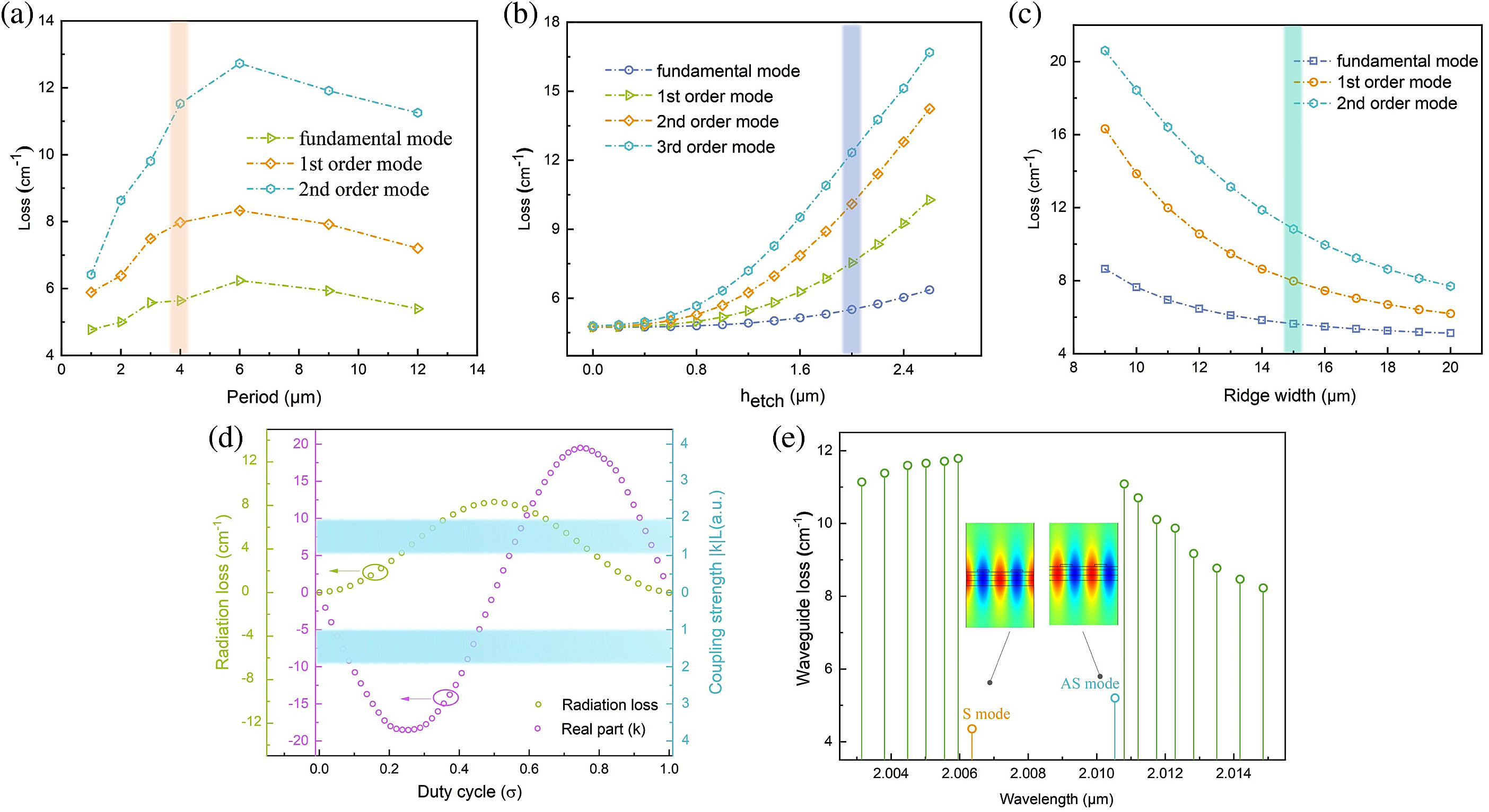
    Fig. 1. The simulation result for the device with corrugated sidewalls and DFB gratings. (a) Waveguide loss of waveguide modes in a waveguide with a full set of corrugated sidewalls, as a function of period of sidewall corrugation. The orange area represents the optimal range selected for the device process etching considering the loss of the fundamental mode and higher-order modes and the feasibility of the process etching. (b) Waveguide loss of waveguide modes in a waveguide with a full set of corrugated sidewalls, as a function of the depth of sidewall corrugation. The gray area represents the optimal range selected for the device process etching considering the loss of the fundamental mode and higher-order modes and the feasibility of the process etching. (c) Waveguide loss of waveguide modes in a waveguide with a full set of device ridge widths, as a function of the ridge width. The cyan area represents the optimal range selected for the device process etching considering the loss of the fundamental mode and higher-order modes and the feasibility of the process etching. (d) The coupling coefficient (gratingdepth=40  nm) changes with the duty cycle. The blue region indicates the optimized coupling strength range (|k|L=12). (e) Mode spectrum for a 2.0 mm long and infinitely wide cavity with DFB gratings (Λ=0.626  μm, σ=45%) computed by finite element analysis. The losses for symmetric and anti-symmetric modes are plotted in orange and blue, respectively, and the losses for various resonant modes of a cavity with a second-order grating other than these two are plotted in green lines. The insets show electric field profiles for symmetric and anti-symmetric modes, respectively.
    (a) 3D cross-sectional model of a 2 μm DFB laser. The inset shows an enlarged view of the buried and corrugated gratings of the device. (b) Scanning electron microscope image of the fabricated 2 μm DFB laser. (c) Top view of the buried grating and corrugated sidewalls. (d) Enlarged view of the buried grating and sidewall grating to verify the dimensions.
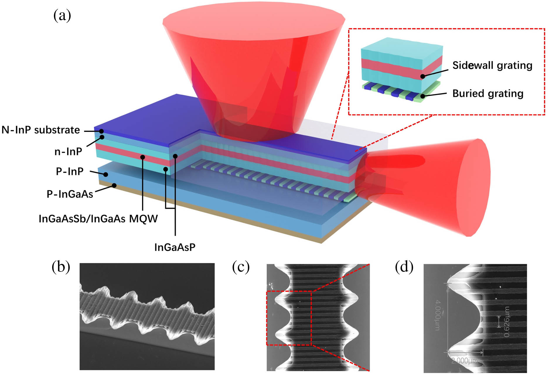
    Fig. 2. (a) 3D cross-sectional model of a 2 μm DFB laser. The inset shows an enlarged view of the buried and corrugated gratings of the device. (b) Scanning electron microscope image of the fabricated 2 μm DFB laser. (c) Top view of the buried grating and corrugated sidewalls. (d) Enlarged view of the buried grating and sidewall grating to verify the dimensions.
    L-I-V characterization of devices with ridge widths of 5, 8, 12, and 15 μm, operating in CW mode at room temperature (300 K).
    Fig. 3. L-I-V characterization of devices with ridge widths of 5, 8, 12, and 15 μm, operating in CW mode at room temperature (300 K).
    CW emission spectra of a second-order DFB laser at different temperatures from 288 to 318 K. (a) CW emission spectra of a second-order DFB laser with ridge widths of 8 μm at different temperatures from 288 to 318 K. The inset shows the lasing spectra under different injection currents at 300 K. (b) CW emission spectra of a second-order DFB laser with ridge widths of 15 μm at different temperatures from 288 to 318 K. The inset shows the lasing spectra under different injection currents at 300 K.
    Fig. 4. CW emission spectra of a second-order DFB laser at different temperatures from 288 to 318 K. (a) CW emission spectra of a second-order DFB laser with ridge widths of 8 μm at different temperatures from 288 to 318 K. The inset shows the lasing spectra under different injection currents at 300 K. (b) CW emission spectra of a second-order DFB laser with ridge widths of 15 μm at different temperatures from 288 to 318 K. The inset shows the lasing spectra under different injection currents at 300 K.
    Far-field profiles of edge emission in the ridge width direction. The circles and squares represent the experimental measurements, which are fitted with Gaussian functions, shown as dashed-dotted lines.
    Fig. 5. Far-field profiles of edge emission in the ridge width direction. The circles and squares represent the experimental measurements, which are fitted with Gaussian functions, shown as dashed-dotted lines.
    Yongqiang Sun, Yunfei Xu, Jinchuan Zhang, Fengmin Chen, Junqi Liu, Shuman Liu, Quanyong Lu, Ning Zhuo, Lijun Wang, Fengqi Liu, Shenqiang Zhai. High-power distributed feedback lasers based on InP corrugated sidewalls at λ∼2 μm[J]. Photonics Research, 2023, 11(8): 1390
    Download Citation