1Key Laboratory of Semiconductor Materials Science, Institute of Semiconductors, Beijing Key Laboratory of Low Dimensional Semiconductor Materials and Devices, Chinese Academy of Sciences, Beijing 100083, China
2Center of Materials Science and Optoelectronics Engineering, University of Chinese Academy of Sciences, Beijing 100049, China
3Beijing Academy of Quantum Information Sciences, Beijing 100193, China
We report a high-power single-mode InP-based 2 μm distributed feedback (DFB) laser with a second-order buried grating and corrugated sidewalls. A second-order semiconductor grating is used for in-plane feedback and vertical out-coupling. The corrugated sidewalls are used to eliminate higher-order transverse modes. For the DFB laser with a 2 mm long cavity and 15 μm wide ridge, the maximum continuous-wave edge-emitting and surface-emitting single-mode powers at 300 K are up to 81 and 42 mW, respectively. A single-lobed far-field radiation pattern with a low divergence angle of approximately 8.6° is achieved by a device with a ridge width of 15 μm. The single-longitudinal-mode emission wavelength of the fabricated laser can be adjusted from 2003.8 nm at 288 K to 2006.9 nm at 313 K without any mode hopping. Robust single-mode emission with a side-mode suppression ratio of 30 dB is achieved under all injection currents and temperature conditions.
1. INTRODUCTION
Semiconductor light sources emitting in the mid-infrared spectral region (2–4 μm) are widely applied in chemical and biological sensing, infrared spectroscopy, and free-space communications because they correspond to the atmospheric window and molecular fingerprint absorption bands [1–6]. To realize these applications, it is necessary to develop stable single-mode high continuous-wave (CW) power and useful beam quality of the above-mentioned light sources, which has been a major aim in the field of photonics. InP-based active-area and GaSb-based active-area structured light sources are the most used devices in the mid-infrared spectral region because of their compactness and reliability [7–10]. In earlier studies, 2 μm single-mode distributed feedback (DFB) devices made of GaSb were the most reported because GaSb-based Fabry–Perot (FP) devices significantly outperformed InP-based devices [11,12]. However, the GaSb-based 2 μm epitaxial wafer contains a high aluminum concentration. Oxidation of aluminum makes conventional fabrication of DFB lasers with regeneration steps technically challenging [8,13]. Gain coupling can be introduced using a laterally coupled DFB (LC-DFB) laser [14–17], achieving high yield and single-mode output. However, additional losses are generated in the laser cavity, so the current best output power of GaSb-based lasers in the world at 283 K is about 40 mW [9,18,19]. Furthermore, it is difficult to regrow crystalline material in a GaSb-based material system. Therefore, the buried DFB grating is hard to fabricate, hindering the improvement of device performance [8,10]. Considering the advantages of low cost, high quality, and process compatibility, the InP material system is becoming more popular compared with the traditional GaSb material system [14]. InP-based lasers are advantageous for a variety of applications, such as vertical-cavity surface-emitting lasers and silicon integrated devices, because the InP material platform is monolithically compatible with many photonic integrated circuits [20–22]. However, in contrast to the 2 μm GaSb laser, the output power of FP devices based on InP substrate is limited to 10 mW [23–25], which significantly affects the performance of the InP-based DFB laser near 2 μm. The InP-based multiple quantum well DFB laser designed by Sato et al. has greatly limited the DFB laser output power due to the large strain mismatch problem [24]. Considering the balance between high power and beam quality of the device being fabricated, the early performances of DFB lasers prepared by our group [22] and Xu et al. [26] did not exceed 20 mW. Therefore, both material growth and device processing greatly resist the performance improvement of DFB devices based on InP. There is still some distance away from the performance of GaSb-based DFB lasers [9,14]. Recently, our group reported promising results for an FP laser diode with emission at hundreds of mW output power [27] by overcoming difficulties such as large lattice mismatch epitaxy and other loss mechanisms [26,28], which demonstrated the potential of InP-based lasers in this wavelength range. On the other hand, inspired by the buried grating technique used in edge-emitting quantum cascade lasers (QCLs), we apply it to a second-order buried grating and corrugated sidewall 2 μm DFB laser to achieve low waveguide loss and high beam quality.
In this paper, we report a high-power single-mode InP-based 2 μm DFB laser with a second-order buried grating and corrugated sidewalls. The second-order semiconductor grating is used for in-plane feedback and vertical out-coupling. The corrugated sidewalls are used to eliminate higher-order transverse modes. The DFB lasers have 2 mm long and 15 μm wide ridge waveguides with a high anti-reflection coating. The maximum CW edge-emitting and surface-emitting single-mode powers at 300 K are up to 81 and 42 mW, respectively. The side-emitting power of this 2 μm laser at 300 K is nearly twice the highest power of the GaSb-based DFB laser at 283 K currently reported internationally [9,17]. The single-longitudinal-mode emission wavelength of the fabricated laser can be adjusted from 2003.8 nm at 288 K to 2006.9 nm at 313 K without any mode hopping. Robust single-mode emission with a side-mode suppression ratio (SMSR) of 30 dB is achieved under all injection currents and temperature conditions.
2. MATERIALS AND METHODS
To prepare for device fabrication, the structures are grown by low-pressure (100 mbar) metal organic chemical vapor deposition with a close-coupled showerhead growth chamber. The group III precursors are trimethylindium [TMIn, In], trimethylgallium [TMGa, Ga], trimethylantimony [TMSb, ], and trimethylaluminum [TMAl, Al], and the group V precursors are arsine () and phosphine (). The n-type dopant precursor is diluted monosilane (), balanced in hydrogen (0.02% in ). The laser structure is grown on an S-doped InP substrate. Figure 2(a) shows a clear picture of the growth structure. First, a 300 nm Si-doped -InP buffer is deposited on the InP substrate at 635°C. A 1000 nm n-InP lower cladding layer and a 100 nm lattice-matched InGaAsP quaternary alloy matrix emitting at 1.1 μm are deposited on an InP substrate at 635°C. Then, the active core is sandwiched between two InGaAsP layers, and the InGaAsP layers are surrounded by upper and bottom InP waveguide layers. The active core consists of three periods of quantum wells and barriers. Compared with previous ideas, we not only re-optimized the growth temperature, but also changed the growth method of the active region [7,22]. Growth temperature is a key factor in large strain epitaxy; the purpose of optimizing temperature is to avoid 3D growth with dislocation and relaxation. The temperature of the heating wire in the reaction chamber was lowered from 635° to 515°C in 5 min. The purpose of stabilizing at this temperature for 3 min is to protect the temperature from overshooting. The active region deposited at 515°C was a multi-quantum well (MQW) () structure with three periods, which contained 5.2 nm thick InGaAs(Sb) wells and 18.9 nm thick InGaAs barriers that were nearly lattice-matched with InP. A growth interruption of 3 s was employed at every InGaAs/InGaAsSb interface while maintaining continuous As flux. These growth interruptions help to reduce compositional grading across the InGaAs/InGaAsSb interfaces [29,30]. Among them, the gallium source and the indium source are turned on and off together, while the antimony source is turned on only when the quantum well is growing. The flow rate of the antimony source is controlled by the source bottle temperature ( to ) and the mass flow controller, which varies from a minimum value to a maximum value. The antimony can inhibit the interdiffusion of atoms, which is beneficial to form a sharper composition interface and enhance the compositional contrast between well barriers, and InGaAsSb quantum wells are formed efficiently. Furthermore, the bandgap will be compressed, resulting in a redshift of the emission wavelength from 2.0 to 2.1 μm [7,22]. Then we return the wafer temperature to 635°C in the same way. A 100 nm InGaAsP layer and a 1200 nm p-InP overlying layer are grown again. Finally, a 200 nm Zn-doped -InGaAs layer is used as the ohmic contact layer.
Sign up for Photonics Research TOC. Get the latest issue of Photonics Research delivered right to you!Sign up now
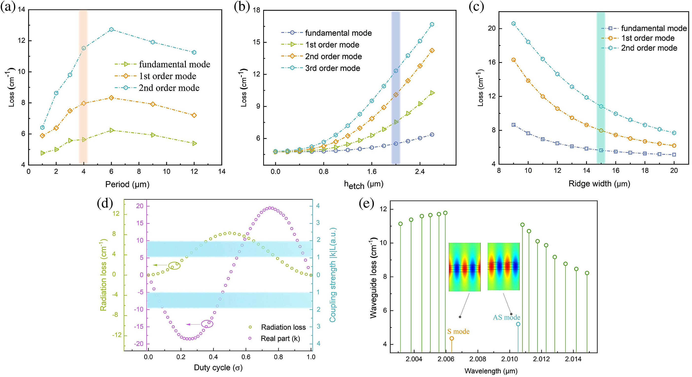
Sidewall gratings not only preferentially generate additional scattering losses for unwanted higher-order lateral modes, but also function as higher-order gratings to facilitate single-longitudinal-mode lasing of the device [10,31]. The relationship between the length of the sidewall grating period and the transverse mode loss is analyzed by finite element simulation. It can be observed from Fig. 1(a) that as the period length of the sidewall grating increases, the loss trends of both high-order modes and the fundamental mode first increase to a certain peak and then decrease. The comparison of the difference between the fundamental transverse mode and the higher-order mode draws our attention, because the fundamental transverse mode of the poorer device is easier to lase when the difference is greater. Therefore, Fig. 1(a) shows that when the length of the sidewall grating is between 3 and 6 μm, the ratio of the loss of the first-order transverse mode to the fundamental transverse mode is between 1.35 and 1.5, which is greater than the ratio of 1.15 in other intervals. To maximize the loss difference between the fundamental and higher-order modes [10,31] and to facilitate the fabrication process, we adopted a sidewall grating with a 50% duty cycle, a period length of 4 μm, and the ratio of 1.5. Moreover, simulations were performed by finite element analysis to examine the loss of lateral modes as a function of the sidewall etching depth and the sidewall grating period length. Figure 1(b) shows how the loss changes in a 15 μm wide waveguide when the etching depth is changed from 0 to 2.6 μm with 0.2 μm increments. As the etching depth gradually increases, the loss difference between the fundamental transverse mode and the higher-order mode gradually increases. An etching depth of 2.0 μm is chosen to secure sufficient loss differences between the fundamental mode and higher-order modes without complicating the fabrication process. In this case, the loss value of the first-order mode is as large as 1.4 times the loss value of the fundamental transverse mode. This enables the fabricated device to easily operate in the fundamental transverse mode.
Figure 1.The simulation result for the device with corrugated sidewalls and DFB gratings. (a) Waveguide loss of waveguide modes in a waveguide with a full set of corrugated sidewalls, as a function of period of sidewall corrugation. The orange area represents the optimal range selected for the device process etching considering the loss of the fundamental mode and higher-order modes and the feasibility of the process etching. (b) Waveguide loss of waveguide modes in a waveguide with a full set of corrugated sidewalls, as a function of the depth of sidewall corrugation. The gray area represents the optimal range selected for the device process etching considering the loss of the fundamental mode and higher-order modes and the feasibility of the process etching. (c) Waveguide loss of waveguide modes in a waveguide with a full set of device ridge widths, as a function of the ridge width. The cyan area represents the optimal range selected for the device process etching considering the loss of the fundamental mode and higher-order modes and the feasibility of the process etching. (d) The coupling coefficient () changes with the duty cycle. The blue region indicates the optimized coupling strength range (). (e) Mode spectrum for a 2.0 mm long and infinitely wide cavity with DFB gratings (μ, ) computed by finite element analysis. The losses for symmetric and anti-symmetric modes are plotted in orange and blue, respectively, and the losses for various resonant modes of a cavity with a second-order grating other than these two are plotted in green lines. The insets show electric field profiles for symmetric and anti-symmetric modes, respectively.
Based on the above results, we simulate the loss of transverse mode by ridge width under sidewall gratings. Figure 1(c) shows the simulation results of the fundamental mode loss and higher-order mode loss for different ridge widths. With the increase of the ridge width, the loss of the fundamental mode is close to the loss of the high-order mode, and the effect of the sidewall grating is gradually weakened. Figure 1(c) shows that when the ridge width is below 16 μm, the ratio of the loss of the first-order mode to the loss of the fundamental transverse mode is above 1.5, and the loss of the high-order mode increases rapidly with the exponential function. After device fabrication, the great beam quality of the laser can be achieved. But above 17 μm, the ratio of the loss of the first-order mode to the loss of the fundamental transverse mode is about 1.18, which is relatively close to one. This will cause the manufactured device to be difficult to lase in the fundamental transverse mode. In the balance between maintaining the maximum output power of the laser and expanding the loss difference between the fundamental transverse mode and the high-order mode, we finally choose a ridge width of 15 μm, as shown in the cyan area in Fig. 1(c).
According to the coupled-wave theory for gratings [32], the feedback in the DFB structure relies on periodic modulation of the refractive index. It is necessary to use numerical analysis to study the mechanism between the working principle of DFB and the grating parameters. Therefore, the system is simulated to find the optimal grating design in the finite element analysis. Furthermore, we address the complex eigenfrequency of the laser by modeling the infinite grating structure () using periodic boundary conditions and grating period . The values of the grating coupling coefficient can be calculated using the expression presented in Ref. [33]: where , , are surface-radiation loss, and the waveguide loss of asymmetric mode and symmetric mode, respectively. is the Bragg wave vector, which equals . The real part of relates to propagating wave vectors and . The imaginary part of relates to the radiation loss in the waveguide [34–36]. Through a series of calculated eigenvalues, the complete is obtained. The values of the real part (index-coupling) of as functions of the grating duty cycle are shown in Fig. 1(d). For surface-emitting devices, it is desirable to maximize the surface radiation component. From Fig. 1(d), the radiation loss reaches the maximum when the duty cycle of the grating is 50%, but the coupling strength is too weak at this condition. Therefore, the blue region in Fig. 1(d) shows that the optimal value of coupling strength () for the most efficient surface emission is 1–2, where is the cavity length [32]. The optimized ranges of the duty cycle () are 0.41–0.46 and 0.56–0.60. Considering the trade-off between surface radiation and stable single-mode operation at high output power, we choose a duty cycle of approximately 45%, where the coupling strength of is approximately 1.68. According to the optimized parameters above, the duty cycle of the grating is 45% and the depth parameters (40 nm) are selected to simulate the loss of the device in the symmetric mode and anti-symmetric mode as a function of wavelength. Figure 1(e) shows that the loss in the symmetric mode is and the loss in the anti-symmetric mode is . The symmetric mode near 2006 nm is less lossy than the anti-symmetric mode, and thus will be the lasing mode. The insets show the electric field profiles for symmetric and anti-symmetric modes of the photonic band structures.
The epitaxial wafer is used to fabricate the lasers, similar to those previously reported [37–39]. First, the second-order grating pattern was obtained by holographic exposure, and the sidewall grating was fabricated by dry etching. These devices were then subjected to secondary epitaxial growth. Double channels were etched and filled with semi-insulating InP:Fe for enhanced heat dissipation around the ridge. Then, a 450 nm thick layer was deposited by plasma enhanced chemical vapor deposition for insulation, and a Ti/Au layer was deposited by electron beam evaporation for electrical contact. An additional 4 μm thick gold layer is electroplated to improve heat dissipation, and a Ge/Au/Ni/Au metal contact layer was deposited on the substrate, which was thinned to 140 μm. The waveguides were then cleaved into 2 mm long bars. The back facet was coated with high-reflectance . In addition, a single layer of was deposited to 270 nm on the front facet, providing 6.7% reflectivity to suppress mode hopping. The double channel ridge structures with average ridge widths of 5, 8, 12, and 15 μm were fabricated by photolithography and wet chemical etching. Because of the anisotropy of two directions, the devices exhibit higher transverse resistivity and less leakage, and thus, the ridge structure were beneficial to reduce electrical loss. To further improve heat dissipation and achieve higher output power, the device was mounted epi-side down on the diamond heatsink with indium, which was subsequently soldered on copper heat sinks. Transverse resistivity and less leakage, and thus, the ridge structure were beneficial to reduce electrical loss.
Figure 2(a) shows a 3D cross-sectional model of a 2 μm DFB laser. The inset shows an enlarged view of the buried and corrugated gratings of the device. According to our simulation, we choose a duty cycle near 45%, which can be controlled by adjusting exposure and developing time, shown in Fig. 2(a). Figure 2(b) shows the scanning electron micrograph of DFB laser ridges with laterally patterned chromium gratings and buried secondary gratings before secondary epitaxy. Figure 2(c) shows the top view of the DFB laser ridge with a clear laterally patterned corrugated grating and buried second-order grating before secondary epitaxy. The second-order grating fabricated by holographic exposure exhibits high quality, which is conducive to single-mode lasing. Figure 2(d) shows the enlarged picture. The periods of the second-order grating and sidewall grating are 626 nm and 4 μm, respectively, and the duty cycle of the sidewall grating is 50%.
Figure 2.(a) 3D cross-sectional model of a 2 μm DFB laser. The inset shows an enlarged view of the buried and corrugated gratings of the device. (b) Scanning electron microscope image of the fabricated 2 μm DFB laser. (c) Top view of the buried grating and corrugated sidewalls. (d) Enlarged view of the buried grating and sidewall grating to verify the dimensions.
The output power of the device was measured using a calibrated thermopile detector with a collection efficiency of nearly 100%. Figure 3 shows the light-current-voltage (L-I-V) characteristics at room temperature (300 K) for 2 mm long devices with ridge widths of 5, 8, 12, and 15 μm. The current was kept lower than the roll-over to prevent the device from burning out. Within the tested current range, Fig. 3 shows that the CW working voltage range is 1.2 to 2.5 V. Although the single-mode operation of the LC-DFB laser is guaranteed, the slope efficiency decreases rapidly with the increase of the coupling degree, resulting in a significant decrease in output power. In addition, as the injection current increases, the laser oscillation becomes unstable, which is prone to occur in multi-mode operation [9,17]. The buried secondary grating will not suffer from the above-mentioned troubles; the performance of the device is greatly improved due to the excellent heat dissipation effect of the semi-insulating Fe-InP. Therefore, at 300 K, the maximum CW optical output power of the device with ridge widths of 15 μm can reach 81 and 42 mW for edge and surface emissions, respectively. The side-emitting power of this 2 μm laser is nearly twice the highest power of the GaSb-based DFB laser currently reported internationally [9]. The SMSR remains as high as 30 dB under peak output power, as shown in Fig. 4 (inset). The edge-emission slope efficiency of at a low injection current and total wall-plug efficiency of can also be calculated from the L-I-V curves. Although the laser ridge width is only 5 μm, the CW edge-emitting output power and the surface-emitting output power are maintained at 8.5 and 4.8 mW, respectively.
Figure 3.L-I-V characterization of devices with ridge widths of 5, 8, 12, and 15 μm, operating in CW mode at room temperature (300 K).
Figure 4.CW emission spectra of a second-order DFB laser at different temperatures from 288 to 318 K. (a) CW emission spectra of a second-order DFB laser with ridge widths of 8 μm at different temperatures from 288 to 318 K. The inset shows the lasing spectra under different injection currents at 300 K. (b) CW emission spectra of a second-order DFB laser with ridge widths of 15 μm at different temperatures from 288 to 318 K. The inset shows the lasing spectra under different injection currents at 300 K.
The spectral characterization was performed using a Fourier transform infrared (FTIR) spectrometer equipped with a deuterated triglycine sulfate detector and a resolution of in rapid scan mode. Figure 4 shows the CW edge-emission spectra of a second-order DFB laser with ridge widths of 8 and 15 μm near the drive current at different temperatures from 288 to 318 K. Figure 4 also shows the spectrum of 8 and 15 μm ridge width lasers from the lasing to inflection point current range. An SMSR of up to 30 dB was achieved, and no mode hopping was observed for the entire temperature range. Since we are using an FTIR spectrometer, the detected wavelengths are located in the edge range of the pyroelectric detector, which will generate thermal noise and limit the size of the SMSR. Figure 4(a) shows that the spectral peak of the laser with 8 μm ridge width was shifted from 4992 to (2003.3 to 2006.4 nm), corresponding to a temperature-tuning coefficient of 0.105 nm/K. The inset shows the lasing spectra obtained under different injection currents at 300 K, and no mode hopping was observed for the entire injection current range. The current tuning rates are similar to our previous report [22]. They are all lower than those reported using epi-up mounts on copper. This indicates the lower thermal resistance obtained by using the epi-down mount [26]. Similarly, the spectral peak of the laser with 15 μm ridge width in Fig. 4(b) was shifted from 4990.5 to (2003.8–2006.9 nm), corresponding to a temperature-tuning coefficient of 0.103 nm/K. The inset also shows that no mode hopping was observed for the entire injection current range. Moreover, single-mode operation is maintained at a relatively high current, and a certain amount of gain/loss coupling is always present in a second-order DFB laser. This loss coupling should prevent the device from oscillating in both stopband modes. Similar devices can be used for trace gas sensing of a substance such as .
The far-field profiles were obtained by placing the laser on a stepped motor control rotational stage with a resolution of 0.1° in the ridge width direction. A nitrogen-cooled HgCdTe detector was located 15 cm away to collect the lasing light. The far-field patterns measured under pulsed mode are shown in Fig. 5, where the circles and squares are measured data, and the dashed-dotted lines are Gaussian fitting curves. The testing is performed at 30 cm away from the laser. The full width at half maximum (FWHM) of the lateral far-field profiles is also indicated. Theoretical calculations show that the lowest threshold gain mode emitted through the surface in a second-order semiconductor/semiconductor grating device is the symmetric mode. Based on the Gaussian fittings, the FWHMs of the devices with ridge widths of 5, 8, 12, and 15 μm are 29.5°, 18.2°, 11.5°, and 8.6°, respectively. According to the single-slit diffraction theory, the diffraction limit angles of the FWHMs of the fundamental mode of the devices with ridge widths of 5, 8, 12, and 15 μm are 30°, 18°, 11.8°, and 9.4°, respectively. These are very close to the measured values and indicate useful beam quality.
Figure 5.Far-field profiles of edge emission in the ridge width direction. The circles and squares represent the experimental measurements, which are fitted with Gaussian functions, shown as dashed-dotted lines.
In conclusion, we have demonstrated the CW operation of a surface-emitting InP-based InGaAsSb/InGaAs quantum well laser. The DFB laser has 2 mm long and 15 μm wide ridge waveguides with high anti-reflection coating. The single-mode CW maximum edge-emitting and surface-emitting output powers at 300 K are 81 and 42 mW, respectively. The side-emitting power of this 2 μm laser is nearly twice the highest power of the GaSb-based DFB laser currently reported internationally. The emission wavelength of the 15 μm wide devices can be adjusted from 2003.8 to 2006.9 nm with a temperature-tuning rate of 0.103 nm/K. A high SMSR of 30 dB is achieved under all injection currents and temperature conditions used herein. Based on the Gaussian fittings, the FWHMs of the devices with ridge widths of 5, 8, 12, and 15 μm are 29.5°, 18.2°, 11.5°, and 8.6°, respectively. These results suggest that the corrugated sidewall grating is reasonable and effective as designed. This high-power single-mode DFB laser can be used in portable and highly integrated sensor systems.
Acknowledgment
Acknowledgment. The authors thank Ping Liang and Ying Hu for their help in device processing.
[30] C. A. Wang, B. Schwarz, D. F. Siriani, L. J. Missaggia, M. K. Connors, T. S. Mansuripur, D. R. Calawa, D. McNulty, M. Nickerson, J. P. Donnelly, K. Creedon, F. Capasso. MOVPE growth of LWIR AlInAs/GaInAs/InP quantum cascade lasers: impact of growth and material quality on laser performance. IEEE J. Sel. Top. Quantum Electron., 23, 1200413(2017).