Key Laboratory for Physical Electronics and Devices of the Ministry of Education, Shaanxi Key Lab of Information Photonic Technique, School of Electronics & Information Engineering, Xi’an Jiaotong University, Xi’an 710049, China
Bo Gao, Tao Chen, Vanthanh Khuat, Jinhai Si, Xun Hou, "Fabrication of grating structures on silicon carbide by femtosecond laser irradiation and wet etching," Chin. Opt. Lett. 14, 021407 (2016)
Copy Citation Text
A method for fabricating deep grating structures on a silicon carbide (SiC) surface by a femtosecond laser and chemical-selective etching is developed. Periodic lines corresponding to laser-induced structure change (LISC) are formed by femtosecond laser irradiation, and then the SiC material in the LISC zone is removed by a mixed solution of hydrofluoric acid and nitric acid to form grating grooves. Grating grooves with a high-aspect ratio of approximately 25 are obtained. To obtain a small grating period, femtosecond laser exposure through a phase mask was used to fabricate grating structures with a 1.07 μm period on the surface of the SiC.
Silicon carbide (SiC) is an attractive semiconductor material for a variety of devices because of the environmental resistance provided by carbon when it is combined with silicon[1]. Devices based on SiC are capable of operating in harsh environments because of the outstanding physical and chemical properties of SiC[2–6]. Fabricating various types of microstructures and nanostructures in SiC has increasingly attracted the interest of researchers owing to their potential applications in microelectronics, optoelectronics, and microchemical and microelectromechanical systems[7–11]. Among these structures, SiC grating structures are highly attractive because of their applicability as diffractive elements and sensors in high-temperature environments[12].
Many approaches for fabricating grating structures in dielectric media have been developed, such as the two-beam holographic method, the focused laser or ion direct-writing method, and reactive ion etching (RIE), to name a few[13–16]. SiC, however, is known to be difficult to micromachine owing to its crystalline structure. The primary method used for micromachining SiC is RIE. However, RIE has disadvantages related to masking for etching purposes, low etching rates, and numerous processing steps[17]. A powerful method, femtosecond laser direct writing, has been employed for micromachining SiC. There are many prominent advantages of femtosecond laser micromachining, such as non-contact processing, fast removal rates, and no need for etch masks[18–24].
However, very little research has been conducted on fabricating SiC gratings using a femtosecond laser. DesAutels et al. fabricated SiC surface and subsurface gratings by direct femtosecond laser writing[1]. When using the femtosecond laser direct-writing technique, it is difficult to fabricate deep grooves, especially those with high-aspect ratios (etched depth divided by groove width) because debris might block the energy transfer to the interior of SiC. Recently, we reported a new method for fabricating SiC through holes with a high-aspect ratio using a femtosecond laser and chemical-selective etching[25,26], during which we achieved a hole depth greater than 200 μm and a hole width less than 40 μm. We expect this technique to be applied in fabricating deep grating structures with a high-aspect ratio.
Sign up for Chinese Optics Letters TOC. Get the latest issue of Chinese Optics Letters delivered right to you!Sign up now
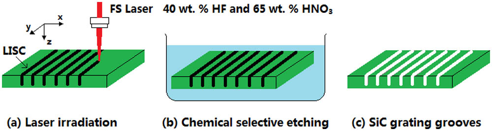
In this Letter, we introduce a new method for fabricating deep grating structures on a SiC surface by a femtosecond laser and chemical-selective etching. The method has two steps: first, periodic lines corresponding to laser-induced structure change (LISC) are formed by femtosecond laser irradiation. Then, a mixed solution of hydrofluoric acid (HF) and nitric acid () is used to remove material in the LISC zone in order to form grating grooves in the SiC. Using this new fabrication method, we obtained grating grooves with a high-aspect ratio of approximately 25. To obtain a small grating period, we used femtosecond laser exposure through a phase mask to fabricate grating structures with a 1.07-μm period on the surface of the SiC. The method has potential applications in the fabrication of grating structures for use in electronic and photonic devices.
A schematic diagram of the fabrication procedure of SiC grating structures with a femtosecond laser and chemical-selective etching is shown in Fig. 1. The experimental setup consisted of a femtosecond laser source, an attenuator, a neutral density filter, a mechanical shutter, an xyz translation stage, a computer, and a CCD camera. The laser source was an amplified Ti:sapphire femtosecond laser system (Libra-USP-HE, Coherent Co. USA) with a pulse duration of 150 fs, a central wavelength of 800 nm, and a repetition rate of 1 kHz. The attenuator provided a convenient way to adjust the laser energy, while the mechanical shutter was employed to control the laser beam access. The sample was mounted on a high-precision translation stage, which was controlled by a computer program.
Figure 1.Schematic diagram of the fabrication of the SiC grating structures.
A 6H-SiC wafer with a thickness of 350 μm was used in our experiments. First, the sample was cleaned using an ultrasonic machine with acetone and then deionized water for 10 min each. Subsequently, the sample was mounted on the translation stage. The laser was adjusted to emit linearly polarized light. The laser beam was focused onto the SiC surface by a microscope objective lens (NA of 0.3, Nikon). The beam diameter of the focus on the sample surface was estimated to be 2.2 μm. During fabrication, the sample surface could be seen either via an optical microscope or on a computer screen connected to the CCD camera. After femtosecond laser irradiation, the side surface of the sample was polished at a random position along the grating in order to observe it from the side. The polished SiC sample was cleaned in an ultrasonic bath with acetone and then with deionized water for 10 min each. Subsequently, the sample was etched with a mixed solution for 60 min. The mixed solution was prepared by mixing 40 wt. % HF and 65 wt. % in a volume ratio of ∶. Then, the SiC sample was again cleaned in an ultrasonic bath with acetone and then with deionized water for 15 min each. Scanning electronic microscopy (SEM) was employed to characterize the morphology of the grating structures before and after etching.
Figure 2 shows cross-section SEM images of the LISC zone and the chemical-selective etching- induced SiC grooves. The average laser power and scanning velocity were set to 5 mW and 7 μm/s, respectively. As shown in Fig. 2(a), LISC zones with depths of 95 μm were formed along the femtosecond laser transmission direction in the irradiated zone. The structural changes in the interior of the SiC were always accompanied by surface ablation. The formation of the LISC zone was attributed to the interaction of the femtosecond laser and the SiC material. The depth of 95 μm was much larger than the Rayleigh length (10 μm) of the focused femtosecond laser. This may be due to the occurrence of the self-trapping of the focused femtosecond laser that leads to long-lasting filaments[26]. After femtosecond laser treatment, the SiC sample was etched with a mixed solution of HF and for 60 min. The LISC zone reacted with the solution and was completely removed, forming funnel-shaped grooves in the SiC, as seen in the cross-sectional images of the SiC in Fig. 2(b). The side walls of the grooves were very smooth. The depth of the grooves was about 95 μm. The width of the grooves was uniform (μ) in the depth range from 20 μm below the surface to the bottom of the grooves. The aspect ratio (completely etched depth divided by groove width at the middle depth) was calculated to be about 25. Notably, only the LISC zone reacted with the acid solution. It is possible that the LISC zone is composed of , Si, and amorphous SiC[26]. The related chemical processes are shown as follows[27,28]: According to above related chemical processes, Eqs. (1)–(3), acts as the oxidizing agent, and HF removes the generated from the laser treatment process. Crystal SiC has good chemical stability and hardly reacts with . Therefore, the materials in the LISC zone were removed, and the surrounding zones remained unchanged. This method demonstrates the high selectivity. By increasing the incident average laser power or decreasing the scanning velocity, we could increase the groove depth and aspect ratio[26]. In addition, the NA characterizes the focus capacity of the lens to the incident laser beam. When a microscope objective lens with a larger NA (such as and microscope objectives and so on) was used, the laser spot size at the focal plane and the Rayleigh length were decreased. The decrease of the laser spot size could result in finer structures. The decrease of the Rayleigh length resulted in the decrease of the LISC length. In addition, the divergence angles of the focused laser beams increased with the increasing NA of the microscope objective lens. The increase of the divergence angles decreased the length of self-trapping and thereby also decreased the length of the LISC zone. Therefore, by using a microscope objective lens with a larger amplification ratio than that for , we could obtain finer structures, but would also obtain shallower grooves.
Figure 2.Cross-section SEM images of the LISC zone (a) before and (b) after chemical-selective etching.
Subsequently, we fabricated grating structures using the above femtosecond laser and chemical-selective etching method. Grooves with a period of 20 μm were fabricated, and SiC grating structures with an area of μμ were constructed. The average laser power and scanning velocity were set to 1.9 mW and 7 μm/s, respectively. The scanning direction was along the -axis, parallel to laser polarization. We observed in Fig. 2(b) that the entrance of a groove was funnel shaped. Hence, we removed approximately 10 μm of SiC material from the top surface by polishing after etching. This treatment was performed to remove the surface damage layer surrounding the irradiated zone in order to obtain grooves with uniform widths. Figure 3(a) shows the top view of the SiC grating structures with an area of μμ, which were measured by an optical microscope with magnification. The average grating depth is 30 μm, as measured from the side view image acquired by an optical microscope with magnification (Fig. 3(b)). We observed that the surface of the grating structures is smooth and that the fabricated SiC grating structures are uniform. To the best of our knowledge, there has been no report on using this method to fabricate a small-period grating on the surface of SiC. Using this method, the fabrication of small-period SiC grating structures with excellent uniformity can be achieved very efficiently and quickly.
Figure 3.SiC grating structures from (a) top view and (b) side view under a microscope.
The above method is suitable for fabricating a deep grating with a long period, but it is difficult to obtain a grating with a submicron period. In order to obtain a smaller grating period, we fabricated SiC grating structures by femtosecond laser exposure through a phase mask. A 10 mm-diameter Gaussian beam was focused by a cylindrical lens through a phase mask onto the bulk materials. The focal length of the cylindrical lens was 25 mm. The phase mask was a self-aligning interferometer that reliably produced a highly repeatable spatially modulated interference field. Using the phase mask, we obtained stable interference patterns easily with ultra-short laser pulses[29,30]. The phase mask had a period of 2.14 μm and was made from a 2 mm-thick UV-grade fused silica slab. The first-order diffracted beams produced an interference pattern in a spatial overlap region behind the phase mask; this pattern was irradiated onto the sample surfaces to form the grating structures[31]. The distance between the sample and phase mask was set to 3 mm. Thus, the diffracted beams of different-order pairs (0, , , etc.) would not overlap spatially resulting from an order walk-off effect[29]. Gratings written with a phase mask were directly observable under a standard optical microscope. The laser power and exposure time were set to 150 mW and 0.1 s, respectively. Figure 4(a) shows the grating structures with a 1.07-μm period on the surface of SiC, as observed under a microscope with magnification; it implies that the submicron structures were induced on the SiC surface.
Figure 4.(a) SiC grating structures with a 1.07 μm period observed under a microscope with magnification. (b) Diffraction pattern of SiC grating structures captured by a camera.
The 1.07 μm grating samples were also etched in the mixed solution. No obvious changes were observed. In this method, the focused beam spot on the focal plane was line shaped and had an elliptic area of μ. For the same input power, the average light intensity at focus for a microscope objective lens was almost a few hundred times higher than that for a cylindrical lens. There was a very different energy density for these two methods. Therefore, the 150 mW femtosecond laser focused by the cylindrical lens may be insufficient to form the LISC inside the SiC and only ablated the SiC surface. When the laser was increased to over 300 mW, the grating structures were destroyed because the grating period was too small. For the grating structures formed by using a phase mask and femtosecond laser irradiation, wet etching may be applicable for increasing the groove depth when the grating period is much larger than 1.07 μm.
Then diffraction effects of the samples fabricated by the above two methods were also characterized by using a 633 nm He–Ne laser. The diffraction pattern was irradiated on a paper screen and then was taken by a camera. The typical diffraction pattern was shown in Fig. 4(b), which corresponds to the sample shown in Fig. 4(a). The 0- and -order diffracted beams can be clearly seen. The higher-order diffractions were absent. The period of the fabricated grating for the former method was much larger than that for the latter. According to the diffraction equation for gratings, the diffraction angle for the former method was smaller than that for the latter. The diffraction angles of the 633 nm light for the samples shown in Figs. 3 and 4 were 1.814° and 36.271°, respectively.
In conclusion, we introduce a method for fabricating deep grating structures on a SiC surface by a femtosecond laser and chemical-selective etching. Periodic lines corresponding to the LISC are formed by femtosecond laser irradiation, and then the SiC material in the LISC zone is removed by a mixed solution of HF and to form grating grooves. Using SEM, the morphologies of the LISC zone and SiC grating grooves are analyzed. The fabricated SiC grating structures are uniform. Grating grooves with a high-aspect ratio of approximately 25 are obtained. In order to obtain a small grating period, we use femtosecond laser exposure through a phase mask and fabricated grating structures with a 1.07-μm period on the surface of SiC. The method has potential applications in the fabrication of grating structures for use in electronic and photonic devices.
Bo Gao, Tao Chen, Vanthanh Khuat, Jinhai Si, Xun Hou, "Fabrication of grating structures on silicon carbide by femtosecond laser irradiation and wet etching," Chin. Opt. Lett. 14, 021407 (2016)