• Journal of Infrared and Millimeter Waves
  • Vol. 42, Issue 2, 197 (2023)
Bo-Wu WANG1, Wei-Hua YU1、2, Yan-Fei HOU3, Qin YU1, Yan SUN4, Wei CHENG4, and Ming ZHOU4、*
Author Affiliations
  • 1Beijing Key Laboratory of Millimeter Wave and Terahertz Technology, Beijing Institute of Technology, Beijing 100081, China
  • 2BIT Chongqing Institute of Microelectronics and Microsystems, Chongqing 400031, China
  • 3Beijing Institute of Radio Measurement, Beijing 100039, China
  • 4Monolithic Integrated Circuits and Modules Laboratory, Nanjing Electronic Devices Institute, Nanjing 210016, China
  • show less
    DOI: 10.11972/j.issn.1001-9014.2023.02.008 Cite this Article
    Bo-Wu WANG, Wei-Hua YU, Yan-Fei HOU, Qin YU, Yan SUN, Wei CHENG, Ming ZHOU. A 33~170 GHz cascode amplifier based on InP DHBT technology[J]. Journal of Infrared and Millimeter Waves, 2023, 42(2): 197 Copy Citation Text show less
    The fT and fmaxof the transistor
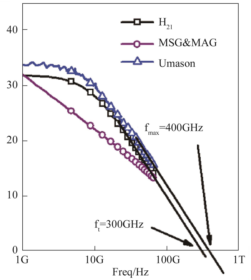
    Fig. 1. The fT and fmaxof the transistor
    Schematic cross-sectional view of (a) multilayer interconnect, and (b) thin-film microstrip lines
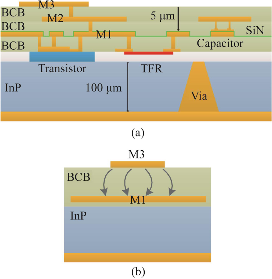
    Fig. 2. Schematic cross-sectional view of (a) multilayer interconnect, and (b) thin-film microstrip lines
    Block diagram of the typical cascode amplifier
    Fig. 3. Block diagram of the typical cascode amplifier
    Circuit topology for the wide band cascode amplifier
    Fig. 4. Circuit topology for the wide band cascode amplifier
    Impedance matching Smith chart and the network schematic
    Fig. 5. Impedance matching Smith chart and the network schematic
    Chip photograph of the cascode amplifier MMIC. Size:1.0 mm × 0.8 mm
    Fig. 6. Chip photograph of the cascode amplifier MMIC. Size:1.0 mm × 0.8 mm
    Measured and simulated S-parameters of the broadband amplifier MMIC On-wafer bias:Vb1=1.5 V,Vb2/Vc=2.5 V
    Fig. 7. Measured and simulated S-parameters of the broadband amplifier MMIC On-wafer bias:Vb1=1.5 V,Vb2/Vc=2.5 V
    Output power measured results
    Fig. 8. Output power measured results
    LayerMaterialThickness/nmDopant
    InP substrate100 µmS.I.
    Emitter contactInGaAs200Si
    EmitterInP200Si
    BaseInGaAs35C
    Setback layerInGaAs30Si
    Step-gradedInGaAsP50Si
    δ-dopingInP5Si
    CollectorInP150Si
    Collector contactInGaAs50Si
    Sub-collectorInP200Si
    Table 1. Layer structure of the InGaAs/InP DHBT
    Ref.. f/GHzTechnologyGain /dBGain Flatness/dBTopology/ DevicesChip-size /mm2Pout/dBm
    140~185500 nm InP DHBT10±2

    Distributed

    ×10

    0.8×0.7510
    40~110100 nm GaAs pHEMT6±2.5

    Cascode

    ×2

    --
    5123~143130 nm SiGe BiCMOS24.3-

    Cascode

    ×10

    0.7×0.437.7
    6110~170SiGe BiCMOS10.8±2.5

    Cascode

    ×2

    0.035-
    7118~23635 nm GaAs mHEMT10-

    Cascode

    ×8

    1.5×0.510
    This work33~170

    500 nm InP

    DHBT

    10±2

    Cascode

    ×2

    1.0×0.81.8
    Table 2. State-of-the-art of ultra-broadband amplifier
    Bo-Wu WANG, Wei-Hua YU, Yan-Fei HOU, Qin YU, Yan SUN, Wei CHENG, Ming ZHOU. A 33~170 GHz cascode amplifier based on InP DHBT technology[J]. Journal of Infrared and Millimeter Waves, 2023, 42(2): 197
    Download Citation