Author Affiliations
1Beijing Key Laboratory of Millimeter Wave and Terahertz Technology, Beijing Institute of Technology, Beijing 100081, China2BIT Chongqing Institute of Microelectronics and Microsystems, Chongqing 400031, China3Beijing Institute of Radio Measurement, Beijing 100039, China4Monolithic Integrated Circuits and Modules Laboratory, Nanjing Electronic Devices Institute, Nanjing 210016, Chinashow less
Abstract
In this paper, a wide band cascode power amplifier working at 33~170 GHz is designed, based on the 500 nm InP dual-heterojunction bipolar transistor (DHBT) process. Two pairs of parallel input and output stub lines can effectively expand the working bandwidth. The output coupling line compensates the high frequency transmission. The measured results show that the maximum gain of the amplifier is 11.98 dB at 115 GHz, the relative bandwidth is 134.98 %, the gain flatness is ±2 dB, the gain is better than 10 dB and the output power is better than 1 dBm in the operating bandwidth.Introduction
With the increasing demand for high data rate and high resolution,it is foreseeable that millimeter wave radar,imaging and communication systems will become are widely applied [1-3]. But at higher frequencies,the achievable gain of tunable amplifiers is low,while distributed amplifiers inherently have wider bandwidths. Therefore the distributed topology is an important way to realize the wide band amplifier. In addition,the cascode amplifier structure also has wide band characteristics and can be used as a basic unit to form a distributed amplifier. The reported cascode amplifiers cover the DC-110 GHz[4],110~170 GHz[5-6],and 140~250 GHz[7] frequency bands,however,designers always have to make a trade-off between bandwidth and gain.
In this paper,an ultra-wideband cascode amplifier operating at 33~170 GHz is demonstrated. The proposed amplifier can achieve 134.98% relative bandwidth and maintain a gain flatness of ±2 dB,with the small signal gain better than 10 dB and the output power better than 1 dBm over the operating bandwidth.
1 InP DHBT technology
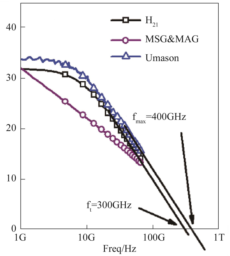
The monolithic microwave integrated circuit(MMIC)was fabricated based on 500-nm dual-heterojunction bipolar transistor(DHBT)process on 3 inch semi-insulating InP substrate using molecular-beam epitaxy(MBE)manufactured by Nanjing Electronic Devices Institute. An InGaAsP composite collector was used to eliminate the current blocking effect caused by the B-C heterojunction conduction band spike[8]. The composite collector area consist of an InGaAs layer,a step-graded InGaAsP layer,and a δ-doping layer,all the layer structures are listed in Table I[9-10]. The width of emitter contact is 500 nm,and two 300 nm wide base contacts at its both side. A transit frequency of 300 GHz and a maximum oscillation frequency above 400 GHz are extracted,as shown in Fig. 1. The process provides three wiring metal layers and compact interconnect vias between them. The MIM capacitor with 0.26 fF/µm2 capacitance density and 25 Ω/square TaN TFR are also available[11].
| Layer | Material | Thickness/nm | Dopant |
|---|
| InP substrate | 100 µm | S.I. |
| Emitter contact | InGaAs | 200 | Si |
| Emitter | InP | 200 | Si |
| Base | InGaAs | 35 | C |
| Setback layer | InGaAs | 30 | Si |
| Step-graded | InGaAsP | 50 | Si |
| δ-doping | InP | 5 | Si |
| Collector | InP | 150 | Si |
| Collector contact | InGaAs | 50 | Si |
| Sub-collector | InP | 200 | Si |
Table 1. Layer structure of the InGaAs/InP DHBT

Figure 1.The fT and fmaxof the transistor
The schematic diagram of the multilayer integrated circuit process used in this paper is shown in Fig. 2. The thickness of the metal layer and corresponding BCB layer are all on the order of 1μm[12]. Each layer of metal can be used as a signal line or a common ground layer. However,when M2 or M3 is used as the ground,the interconnection structures are more complicated and will bring more parasitic mode effects. Therefore,M1 is used as the common ground,in which case only the windows around the series capacitors are opened that will greatly reduce the leak area[13]. Thin-film micro-strip lines(TFMLs)can be realized with M1 as ground and M3 for signal line shown in Fig. 2(b). The effective dielectric thickness is only a few micro-meters,and for a 50 ohm TFML,its line width is almost 12 μm in the band of 1~300 GHz[14].
Figure 2.Schematic cross-sectional view of (a) multilayer interconnect, and (b) thin-film microstrip lines
2 Circuit design
Figure 3 shows the block diagram of a typical cascode amplifier. The common-emitter(CE)HBT produces the controlled output current,this controlled current flows into the common-base(CB)HBT and is buffered by the(CB)HBT. The buffer effect reduces the output resistance of(CE)HBT and reduce the voltage gain of(CE)HBT,which in turn reduces the Miller effect. Such structure has the benefits of better gain while maintaining good linearity and reverse isolation.
Figure 3.Block diagram of the typical cascode amplifier
Figure 4 shows the circuit topology for the designed cascode amplifier. In order to obtain wide bandwidth,two pair parallel open-ended stubs were respectively added to the input matching networks of the first stage(CE)HBT and the output matching networks of the second stage(CB)HBT. One pair of stubs is designed at the higher frequency band,and the other pair is designed at the lower frequency band. Figure 5 shows the amplifier’s optimum power input and output impedance matching network schematics. This makes a trade-off between bandwidth and gain of the amplifier. The folded coupling lines act as parts of matching network while compensating some high frequency transmission loss. An impedance matching line with a width of 20 µm and a length of 250 µm was introduced between the two HBT devices. Since both(CE)HBT and(CB)HBT are supplied by Vc,then the stability of the cascode amplifier is sensitive to the current(the controlled CE output current)passing through the inter-stage matching line. Figure 6 shows this chip photograph of the cascode amplifier MMIC. The size is 1.0 mm × 0.8 mm.
Figure 4.Circuit topology for the wide band cascode amplifier
Figure 5.Impedance matching Smith chart and the network schematic
Figure 6.Chip photograph of the cascode amplifier MMIC. Size:1.0 mm × 0.8 mm
3 On-wafer measurement
Characterization of the MMIC cascode amplifiers were obtained by on-wafer measurements. The measured results are shown in Fig. 7 and Fig. 8. The S-parameter measurements were performed using a Keysight PNA-X N5247B network analyzer with Keysight N5293AX01(1~110 GHz)frequency extenders,and Rohde & Schwarz ZVA50 network analyzer with Rohde & Schwarz ZC170(110~170 GHz)frequency extenders.
Figure 7.Measured and simulated S-parameters of the broadband amplifier MMIC On-wafer bias:Vb1=1.5 V,Vb2/Vc=2.5 V
Figure 8.Output power measured results
The measured results show that the maximum gain of the amplifier at 115 GHz is 11.98 dB,and the 3 dB bandwidth is 33 to 170 GHz(134.98%). Figure 7 also shows the simulation results of no stub or matched impedance line. Through comparison,it can be found that these stubs and matching lines can effectively increase the amplifier bandwidth. Signal fluctuations in the range of 65~85 GHz and 100~110 GHz are large,which is caused by overheating of the frequency extender modules for a long time. The spectrum spurs can be reduced by turning off the system and cooling,but it cannot be completely eliminated. The saturated output power of the device is 1.8 dBm at 117 GHz,when the input power is -5 dBm. The output power is better than 1 dBm in the range of 35~134 GHz,and greater than 0 dBm in the range of 41~170 GHz,as shown in Fig. 7. Accordingly,the output collector current is 5 mA at 2.5V supply and the peak power added efficiency(PAE)is 8.8%.
| Ref. | . f/GHz | Technology | Gain /dB | Gain Flatness/dB | Topology/ Devices | Chip-size /mm2 | Pout/dBm |
|---|
| [1] | 40~185 | 500 nm InP DHBT | 10 | ±2 | Distributed ×10 | 0.8×0.75 | 10 |
| [4] | 0~110 | 100 nm GaAs pHEMT | 6 | ±2.5 | Cascode ×2 | - | - |
| [5] | 123~143 | 130 nm SiGe BiCMOS | 24.3 | - | Cascode ×10 | 0.7×0.43 | 7.7 |
| [6] | 110~170 | SiGe BiCMOS | 10.8 | ±2.5 | Cascode ×2 | 0.035 | - |
| [7] | 118~236 | 35 nm GaAs mHEMT | 10 | - | Cascode ×8 | 1.5×0.5 | 10 |
| This work | 33~170 | 500 nm InP DHBT | 10 | ±2 | Cascode ×2 | 1.0×0.8 | 1.8 |
Table 2. State-of-the-art of ultra-broadband amplifier
Table 2 shows the performance comparison of several wide band amplifiers. We noticed that this design provides the considerable gain,output power and bandwidth characteristics.
4 Conclusion
In this paper,a wide band amplifier is presented,which exhibits a good operating bandwidth(better than 1 dBm in the range of 35~134 GHz). The high 134.98% relative bandwidth completely covers the Q,V,W and D bands,which makes it a suitable option for measurement and spectroscopic systems. In the future,the cascode amplifier shown in this paper can be used as a cell to achieve greater output power through power combining.
References
[1] T Shivan, M Hossain, I D Stoppel et al. An ultra-broadband low-noise distributed amplifier in InP DHBT technology, 1209-1212(2018).
[2] Fei YANG, Heng-Fei ZHAO, Jiang-Tao LIU et al. Solid-state power amplifiers for space: going to extremely high frequency. J. Infrared Millim. Waves, 40, 25-32(2021).
[3] Ying-Hui ZHONG, Kai-Kai LI, Xin-Jian LI et al. A W-band high-gain and low-noise amplifier MMIC using InP-based HEMTs. J. Infrared Millim. Waves, 34, 668-672(2015).
[4] P Shinghal, C I Duff, R Sloan et al. Cascode cell analysis for ultra-broadband GaAs MMIC component design applications, 1-4(2013).
[5] D Hou, Y Xiong, W Goh et al. A D-band cascode amplifier with 24.3 dB gain and 7.7 dBm output power in 0.13 $\mu$m SiGe BiCMOS technology. IEEE Microwave and Wireless Components Letters, 22, 191-193(2012).
[6] I Petricli, H Lotfi, A Mazzanti. Analysis and design of D-Band cascode SiGe BiCMOS amplifiers with gain-bandwidth product enhanced by load reflection. IEEE Transactions on Microwave Theory and Techniques, 69, 4059-4068(2021).
[7] B Amado-Rey, Y Campos-Roca, C Friesicke et al. A G -band broadband balanced power amplifier module based on cascode mHEMTs. IEEE Microwave and Wireless Components Letters, 28, 924-926(2018).
[8] W Cheng, Z Jin, Y B Su et al. Composite-collector InGaAs/InP double heterostructure bipolar transistors with current-gain cutoff frequency of 242 GHz. Chinese Physics Letters, 26, 038502(2009).
[9] Wei CHENG, You-Tao ZHANG, Yuan WANG et al. 0.5μm InP DHBT technology for 100GHz+ mixed signal integrated circuits. J. Infrared Millim. Waves, 36, 167-172(2017).
[10] Bin NIU, Wei CHEN, You-Tao ZHANG et al. 0.5 μm InP/InGaAs DHBT for ultra high speed digital integrated circuit. J. Infrared Millim.Waves, 35, 263-266(2016).
[11] O P Li, Y Zhang, T D Zhang et al. 140 GHz power amplifier based on 0.5 µm composite collector InP DHBT. IEICE Electronics Express, 14, 20170191(2017).
[12] K Eriksson, S E Gunnarsson, P Nilsson et al. Suppression of parasitic substrate modes in multilayer integrated circuits. IEEE Transactions on Electromagnetic Compatibility, 57, 591-594(2015).
[13] Yan-Fei HOU, Bo-Wu WANG, Wei-Hua YU et al. Parasitic modes caused by defect ground structure in multilayer integrated circuit. Journal of Terahertz Science and Electronic Information Technology, 20, 626-630(2022).
[14] Y P Chen, Y Zhang, Y H Xu et al. Investigation of terahertz 3D EM simulation on device modeling and a new InP HBT dispersive inter-electrode impedance extraction method. IEEE Access, 6, 45772-45781(2018).