
Jianliang Huang, Chengcheng Zhao, Biying Nie, Shiyu Xie, Dominic C. M. Kwan, Xiao Meng, Yanhua Zhang, Diana L. Huffaker, Wenquan Ma, "High-performance mid-wavelength InAs avalanche photodiode using AlAs0.13Sb0.87 as the multiplication layer," Photonics Res. 8, 755 (2020)
- Photonics Research
- Vol. 8, Issue 5, 755 (2020)
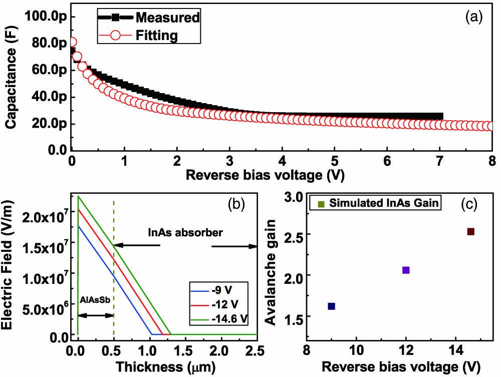
Fig. 1. (a) C-V measured at room temperature with the fitting. The device size is 400 μm × 400 μm

Fig. 2. (a) Dark current curves of a device with a mesa area of 400 μm × 400 μm
Fig. 3. (a) Arrhenius plot of the dark current for the temperature range between 77 and 275 K. (b) Activation energy versus the forward bias voltage. (c) Dependence of the ( 1 / R 0 A ) − 1 ( p / A ) − 1
Fig. 4. Measured responsivity under different bias voltages at room temperature. The responsivity of the reference device is also shown.
Fig. 5. Avalanche gain with respect to the reverse bias voltage. The inset is the responsivity with respect to the reverse bias voltage for different wavelengths.
Fig. 6. (a) Measured NEP of the device with respect to wavelength at different reverse bias voltages with the inset showing the measured noise current. (b) The corresponding D ⋆ 400 μm × 400 μm
| ||||||||||||||||||||||||||||||||||
Table 1. Details of the Device Structure


Set citation alerts for the article
Please enter your email address

© Copyright 2018-2021 | Chinese Laser Press. All Rights Reserved 沪ICP备15018463号-20