Abstract
We report on a high-performance mid-wavelength infrared avalanche photodetector (APD) with separate absorption and multiplication regions. InAs is used as the absorber material and high-bandgap is used as the multiplication material. At room temperature, the APD’s peak response wavelength is 3.27 μm, and the 50% cutoff wavelength is 3.5 μm. The avalanche gain reaches 13.1 and the responsivity is 8.09 A/W at 3.27 μm when the applied reverse bias voltage is 14.6 V. The measured peak detectivity of the device is at 3.27 μm.1. INTRODUCTION
Mid-wavelength (MW) infared photodetectors are widely needed in military and civil applications. Currently, commercially available high-performance MW detectors are mainly based on HgCdTe [1], InSb [2], and PbS/PbSe [3] materials. To detect very weak and even single-photon signals [4], an avalanche photodetector (APD) is by far the most widely used device due to its high internal gain. To obtain high performance, it requires a low to minimize the excess noise of an APD. , where and are the impact ionization coefficient of electron and hole, respectively. The lower the , the smaller the excess noise factor [5]. In this respect, HgCdTe is an ideal APD material in the MW range because its is close to zero [6]. However, this material also has some drawbacks in terms of APD application. For instance, HgCdTe material suffers from the so-called composition nonuniformity problem. Moreover, a CdZnTe substrate for high-performance APD is of high cost, and its large size growth is still a challenge. Another ideal material for MW APD is InAs [7]. On the one hand, its bandgap is in the MW range, and its value is about 0.41 eV at 77 K and 0.35 eV at 300 K. On the other hand, it has been reported that its is also very close to zero [8,9], and it can achieve sole electron multiplication with a very small excess noise factor [10]. In spite of these positive features, there are still some hurdles to overcome. First, a large electric field, which is required to achieve high gain, may cause high tunneling dark current in this narrow-bandgap material. Second, to realize a high internal gain, the thickness of the InAs APD should be as large as 10 μm [4,9], and the background carrier concentration should be as low as [11,12]. This poses a serious challenge for the state-of-the-art growth technique. In addition, most of the MW APDs mentioned above need cryogenic cooling to achieve high performance, and this definitely increases the detector’s weight and cost.
In this paper, we report on an MW APD with separate absorption and multiplication regions. InAs is used as the absorber material, and high-bandgap is used as the multiplication material. The APD is of high performance. At room temperature, the APD’s avalanche gain reaches 13.1, and the responsivity is 8.09 A/W at the peak response wavelength of 3.27 μm when the applied reverse bias voltage is 14.6 V. The shot-noise-limited detectivity of the device is at the peak response wavelength, while the measured peak is . It is analyzed that the APD’s avalanche gain is mainly from AlAsSb rather than InAs. However, when increasing the reverse bias voltage, the InAs’s contribution to the avalanche process is increased.
2. DESIGN AND DEVICE FABRICATION
Table 1 shows the designed APD structure. The design uses separate absorption and multiplication regions, InAs is used as the absorber material, and high-bandgap AlAsSb is used as the multiplication material. The AlAsSb material, which can be lattice-matched to InAs by tuning the Sb composition, has a large indirect bandgap of 2.035 eV [13]. Therefore, AlAsSb can be used to block the tunneling dark current [14,15]. It has been demonstrated that has a large difference between and with of only about 0.005 [16–18]. This low is ascribed to the low because of high phonon scattering rates and large hole effective mass associated with the large Sb composition [19]. Therefore, AlAsSb can be an ideal multiplication material for APD based on the assumption that it has a similar low excess noise performance to that of lattice-matched to InP. By using the design with separate absorption and multiplication regions, the APD’s thickness can be decreased a lot. Specifically, along the growth direction, the bottom -type contact region is a 0.8 μm thick InAs layer doped to using Si, the avalanche multiplication region is a 0.5 μm thick unintentionally doped AlAsSb layer, and the APD absorber is a 2.0 μm thick InAs layer. Finally, the top -type contact region is a 0.5 μm thick InAs layer doped to using Be.
Sign up for Photonics Research TOC. Get the latest issue of Photonics Research delivered right to you!Sign up now
| Material | Design | Modelled |
| Thickness (μm) | Doping (cm−3) | Thickness (μm) | Doping (cm−3) |
| InAs | 0.5 | 2.0 × 10¹⁸(p) | / | 2.0 × 10¹⁸ |
| InAs | 2.0 | Undoped | 2.0 | 1.5 × 10¹⁶ |
| AlAsSb | 0.5 | Undoped | 0.5 | 1.5 × 10¹⁶ |
| InAs | 0.8 | 2.0 × 10¹⁸(n) | / | 2.0 × 10¹⁸ |
| N+ InAs substrate |
Table 1. Details of the Device Structure
The sample is grown on an epi-ready -doped InAs (001) substrate by molecular beam epitaxy using and . The substrate is first heated to 500°C to desorb the native oxide. Then the substrate is cooled down to 450°C to grow the designed structure. After growth, the as-grown sample is processed into square mesas with widths ranging from 200 to 500 μm by photolithography and wet chemical etching. The mesa structure is not surface passivated. Ti (100 nm)/Au (300 nm) alloy is used as both the - and -type ohmic contact metal.
3. RESULTS AND DISCUSSION
The as-grown sample is characterized by high-resolution X-ray diffraction (XRD) measurement with the scan around the InAs (004) reflection using an open detector. The full width at half-maximum of the XRD AlAsSb (004) peak is about 150 arcsec. The AlAsSb (004) peak is at the low-angle side of the InAs (004) substrate peak, and this indicates a compressive strain. The strain is calculated to be about from the spacing between the InAs substrate peak and the AlAsSb peak. Assuming a coherent growth, the As and Sb mole fractions of the AlAsSb layer are calculated to be 13% and 87%, respectively, which are very close to our design of . The carrier concentration of different layers is measured by the capacitance-voltage (C-V) profiling, and Fig. 1(a) shows the result at room temperature. The obtained residual carrier concentration is both for the InAs absorber layer and the AlAsSb multiplication layer. The carrier concentration values of the different layers are also shown in Table 1.
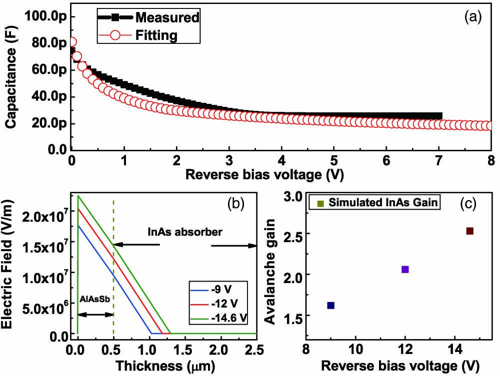
Figure 1.(a) C-V measured at room temperature with the fitting. The device size is . (b) Simulated electric field distribution at different bias voltages. (c) Simulated avalanche gain with respect to the reverse bias voltage.
Figure 2(a) shows the dark current curves of a device with mesa size of for the temperature range from 77 K to 300 K. At 77 K, when the reverse bias voltage is smaller than about 10.5 V, the dark current stays nearly unchanged, and it is dominated by the background-induced photocurrent owing to insufficient shielding. When the applied reverse bias voltage is larger than 10.5 V, the dark current increases exponentially. By fitting the dark current curve for the reverse bias voltage between 10.5 and 18 V [see Fig. 2(b)], it is found that this exponential increase of the dark current is induced by the band-to-band tunneling current in the InAs material, and no avalanche breakdown behavior is observed in our device. The onset of the tunneling current starts at the reverse voltage , corresponding to the peak electric field of 68 kV/cm. This result suggests that, if a proper charge sheet layer is included for the future device design, the electric field distribution in the InAs layer may be reduced, and thus the band-to-band tunneling current can be further reduced.

Figure 2.(a) Dark current curves of a device with a mesa area of for the temperature range from 77 to 300 K. (b) Measured dark current together with the band-to-band tunneling current and the simulated dark current for the bias voltage between 10.5 and 18 V.
The activation energy can be derived from temperature-dependent dark current data. Figure 3(a) shows the Arrhenius plot of the measured dark current for the temperature range between 77 K and 275 K. For the temperature range between 150 K and 300 K, is 0.33 eV, which equals the value of InAs bandgap at room temperature. This implies that the dark current is dominated by the diffusion current. For the temperature range between 110 K and 130 K, is calculated to be 0.17 eV, which is about a half of the InAs bandgap, and this indicates that the dark current is dominated by the generation-recombination current. When the temperature is between 77 K and 100 K, the is only 38 meV. One possibility is that the dark current for this temperature range may originate from some trap-assisted tunneling current. Figure 3(b) shows the dependence of the extracted on the forward bias voltage. By linearly extrapolating the data to the axis, the conduction band offset between InAs and AlAsSb is estimated to be as large as 1.92 eV, which is in agreement with the value of the conduction band offset between InAs and [13]. This result suggests that, if there is a proper grading layer in between InAs and AlAsSb, the electron transport may be facilitated.
Figure 3.(a) Arrhenius plot of the dark current for the temperature range between 77 and 275 K. (b) Activation energy versus the forward bias voltage. (c) Dependence of the on the for different mesa sizes at room temperature.
The dark current is measured for variable mesa sizes (, , , and ). Figure 3(c) is the measured dependence of the on the for different mesa sizes at 300 K, where is the mesa area, is the mesa perimeter, is the resistance-and-area product at zero bias, and is the perimeter-to-area ratio. From the intercept of the fitting line with the vertical axis, the bulk part of is calculated to be . From the slope of the fitting line, the surface resistivity is obtained to be . The variable-mesa-size measurements indicate that the surface leakage current is the dominant part of the dark current at room temperature [20]. For example, the surface leakage current contributes 78% of the dark current where the device area is . This is understandable considering that our device is not surface passivated.
The spectral response of the device is measured by Fourier transform infrared spectroscopy. Then we measure the blackbody response with the blackbody temperature set at 900 K and use this blackbody response to calibrate the spectral response. In this way, we get the wavelength-dependent responsivity. During the measurement, phase-sensitive detection of the photocurrent (chopped blackbody beam and SRS SR830 lock-in amplifier) is employed to minimize the influence of the dark current and the background noise on the photocurrent. Here we also use a commercial InAs photodiode [21] as a reference to calibrate the optical power and spectra of our system. Figure 4 shows the measured responsivity under different bias voltages at room temperature. It can be seen that the 50% cutoff wavelength of the device is 3.5 μm, which corresponds to the bandgap of InAs material of 0.35 eV at 300 K. The peak response is at 3.27 μm, and the responsivity is 0.62, 1.20, and 8.09 A/W when the applied reverse bias voltage is 7.63, 12.1, and 14.6 V, respectively, which corresponds to the external quantum efficiency of 23.5%, 45.5%, and 306.8%, respectively. The responsivity spectrum of the commercial InAs photodiode is also shown in Fig. 4.
Figure 4.Measured responsivity under different bias voltages at room temperature. The responsivity of the reference device is also shown.
The inset of Fig. 5 shows the responsivity with respect to the applied reverse bias voltage for different wavelengths. It can be seen that when the bias voltage is increased from 0.98 to 7.63 V, the responsivity is increased. This increase is due to the enhanced tunneling probability of photogenerated electrons between InAs and AlAsSb when the bias voltage is increased. When the bias voltage is between 7.63 and 9.28 V, the responsivity is found to be like a plateau. With the increasing bias voltage beyond 9.28 V, the responsivity is increased further, and this increase is caused by the avalanche effect. Therefore, the bias voltage of 7.63 V is selected as a reference point to calculate the avalanche gain. Figure 5 is the calculated avalanche gain (M) with respect to the reverse bias voltage for different wavelengths. The avalanche gain reaches 13.1 at 3.27 μm when the bias voltage is 14.6 V. Here the maximum gain measured is limited by the high dark current at room temperature, leading to the appearance of the “saturate” avalanche gain. The avalanche gain also can be confirmed from the dark current data. At 77 K, as shown in Fig. 2(b), there is a difference between the measured dark current and the simulated InAs band-to-band tunneling current. The simulated band-to-band tunneling current is smaller than the measured dark current when the reverse bias voltage is larger than 18.0 V. Using the same method mentioned above, we can get the multiplication gain at 77 K. Using this multiplication gain, the measured dark current at 77 K can be very well fitted. This indicates that the difference is caused by the multiplication effect.
Figure 5.Avalanche gain with respect to the reverse bias voltage. The inset is the responsivity with respect to the reverse bias voltage for different wavelengths.
As can be seen from Fig. 5, for a constant bias voltage, the gain stays the same for different wavelengths when the bias voltage is smaller than 14.1 V. However, when the bias voltage is larger than 14.1 V, the gain changes slightly with respect to wavelength. For example, the gain is 12.9, 12.8, 12.1, 12.4, and 13.1 for 1.3, 1.5, 2.0, 2.5, and 3.27 μm, respectively. To account for this phenomenon, we should analyze which material, InAs or AlAsSb, the avalanche gain arises from. This can be known by simulating the electron field distribution using the device structure, and the carrier density data obtained from the C-V results at room temperature are shown in Fig. 1(b). The simulation was performed assuming that the maximum of the electric field is at the AlAsSb side. The depletion layer thickness is 1.03, 1.18, and 1.30 μm when the bias voltage is 9, 12, and 14.6 V, respectively. It can be seen that the electric field is predominantly distributed in the AlAsSb layer. This implies that the avalanche gain is mainly from the AlAsSb layer. In addition, based on the local model, by knowing the electric field distribution in the InAs layer, we can simulate the avalanche gain that the InAs layer contributes to. The result is shown in Fig. 1(c). The avalanche gain from InAs layer is small when the bias voltage is smaller than 14.1 V, and it is 1.62 and 2.06 when the bias voltage is 9 and 12 V, respectively. However, the avalanche gain from the InAs layer reaches 2.53 when the bias voltage is 14.6 V. This means that, when a large bias voltage is applied, the InAs layer also plays a role in the avalanche process, but still, the avalanche effect predominantly comes from AlAsSb rather than InAs. The contributions from both AlAsSb and InAs make the avalanche gain slightly changed with respect to wavelength under a large bias voltage.
After obtaining the data of the responsivity, dark current, and gain, the shot-noise-limited detectivity of the device can be calculated by [22] where is the responsivity, is the electron charge, is the surface dark current density, is the bulk dark current density with gain of 1, is the product of the dynamic resistance and area, is the Boltzmann constant, is the temperature, and is the avalanche gain. is the excess noise factor and can be expressed as . Here the is estimated to be 0.05 according to Ref. [23]. When M is 10, F(M) is about 2.3. is extracted from the dark current data and is about . is roughly equal to 78% of the measured dark current density. The obtained is at the peak response wavelength of 3.27 μm at 300 K. When M is 1, the obtained is . The of the device is also measured at room temperature. The noise spectra () of the device (bandwidth up to 13.5 kHz) are measured by a spectrum analyzer together with transimpedance amplifier [24]. The result of the noise current at different reverse bias voltages is shown in the inset of Fig. 6(a). Using the values of and , the noise equivalent power (NEP) spectra at different reverse bias voltages are obtained according to , which are shown in Fig. 6(a). The experimental is calculated by , and the result is shown in Fig. 6(b). At 3.27 μm, the measured peak is at reverse bias voltage of 14.4 V at 300 K. It can be seen that the measured peak is about one-seventh of the calculated at M of 10. This might be due to the degradation of device dark current after exposure in the atmosphere environment for more than two years. This suggests that a good passivation layer is necessary for our device for long-term application.
Figure 6.(a) Measured NEP of the device with respect to wavelength at different reverse bias voltages with the inset showing the measured noise current. (b) The corresponding with respect to wavelength. The device size is .
This APD’s performance is very encouraging. We can compare it with some of the state-of-the-art commercial and reported MW APDs. When the gain is 1, the responsivity of our APD is 0.62 A/W, which is smaller than that of Judson’s [25] and Hamamatsu’s InAs APDs [26]. In particular, it is smaller than the result of the InAs APD reported by the Sheffield group [22], which may be the best result reported. However, when the bias voltage is increased to 14.6 V, our APD’s responsivity reaches 8.09 A/W with gain of 13.1, which is already larger than that of the two commercial InAs APDs but is still smaller than that of the APD reported by the Sheffield group. The gain of the Sheffield InAs APD can be as large as 200, and the responsivity can be larger than 300 A/W [27]. However, the thickness of the Sheffield InAs APD is 8 μm, which is much thicker than ours. Moreover, that device’s performance requires a background carrier density as low as . Both the large device thickness and low background carrier density pose a challenge for most of the present growth techniques. In terms of the detectivity, our APD is comparable to the three InAs APDs mentioned above. We should mention that there is still plenty of room to enhance the APD’s performance by effectively surface passivating the device and by optimizing the device design, for example, with the charge sheet layer and the grading layer schemes mentioned above.
4. CONCLUSION
We have demonstrated a high-performance MW APD with separate absorption and multiplication regions. At room temperature, the avalanche gain reaches 13.1, and the responsivity is 8.09 A/W at the peak response wavelength of 3.27 μm when the applied reverse bias voltage is 14.6 V. The measured peak detectivity of the device is at 3.27 μm. Our work may provide a new design method to achieve high-performance APD with reduced device thickness.
References
[1] J. Beck, T. Welch, P. Mitra, K. Reiff, X. Sun, J. Abshire. A highly sensitive multi-element HgCdTe e-APD detector for IPDA lidar applications. J. Electron. Mater., 43, 2970-2977(2014).
[2] J. Abautret, J. P. Perez, A. Evirgen, J. Rothman, A. Cordat, P. Christol. Characterization of midwave infrared InSb avalanche photodiode. J. Appl. Phys., 117, 244502(2015).
[3] A. Rogalski. Recent progress in infrared detector technologies. Infrared Phys. Technol., 54, 136-154(2010).
[4] C. H. Tan, A. Velichko, L. W. L. J. S. Ng. Few-photon detection using InAs avalanche photodiodes. Opt. Express, 27, 5835-5842(2019).
[5] R. J. McIntyre. Multiplication noise in uniform avalanche diodes. IEEE Trans. Electron Devices, 13, 164-168(1966).
[6] J. Beck, C. Wan, M. Kinch, J. Robinson, P. Mitra, R. Scritchfield, F. Ma, J. Campbell. The HgCdTe electron avalanche photodiode. J. Electron. Mater., 35, 1166-1173(2006).
[7] W. L. Sun, Z. W. Lu, X. G. Zheng, J. C. Campbell, S. J. Maddox, H. P. Nair, S. R. Bank. High-gain InAs avalanche photodiodes. IEEE J. Quantum Electron., 49, 154-161(2013).
[8] A. R. J. Marshall, C. H. Tan, M. J. Steer, J. P. R. David. Electron dominated impact ionization and avalanche gain characteristics in InAs photodiodes. Appl. Phys. Lett., 93, 111107(2008).
[9] A. R. J. Marshall, J. P. R. David, C. H. Tan, M. J. Steer. Impact ionization in InAs electron avalanche photodiode. IEEE Trans. Electron Devices, 57, 2631-2638(2010).
[10] A. R. J. Marshall, C. H. Tan, M. J. Steer, J. P. R. David. Extremely low excess noise in InAs electron avalanche photodiodes. IEEE Photonics Technol. Lett., 21, 866-868(2009).
[11] P. J. Ker, A. R. J. Marshall, J. P. R. David, C. H. Tan. Low noise high responsivity InAs electron avalanche photodiodes for infrared sensing. Phys. Status Solidi C, 9, 310-313(2012).
[12] X. X. Zhou, J. S. Ng, C. H. Tan. InAs photodiode for low temperature sensing. Proc. SPIE, 9639, 963901(2015).
[13] I. Vurgaftman, J. R. Meyer, L. R. Ram-Mohan. Band parameters for III-V compound semiconductors and their alloys. J. Appl. Phys., 89, 5815-5875(2001).
[14] W. L. Sun, S. J. Maddox, S. R. Bank, J. C. Campbell. Room temperature high-gain InAs/AlAsSb avalanche photodiode. IEEE Photonics Conference, 350-351(2014).
[15] P. J. Ker, J. P. R. David, C. H. Tan. Temperature dependence of gain and excess noise in InAs electron avalanche photodiodes. Opt. Express, 20, 29568-29576(2012).
[16] C. H. Tan, S. Y. Xie, J. J. Xie. Low noise avalanche photodiodes incorporating a 40 nm AlAsSb avalanche region. IEEE J. Quantum Electron., 48, 36-41(2016).
[17] X. Yi, S. Y. Xie, B. L. Liang, L. W. Lim, X. X. Zhou, M. C. Debnath, D. L. Huffaker, C. H. Tan, J. P. R. David. Demonstration of large ionization coefficient ratio in AlAs0.56Sb0.44 lattice matched to InP. Sci. Rep., 8, 9107(2018).
[18] X. Yi, S. Y. Xie, B. L. Liang, L. W. Lim, J. S. Cheong, M. C. Debnath, D. L. Huffaker, C. H. Tan, J. P. R. David. Extremely low excess noise and high sensitivity AlAs0.56Sb0.44 avalanche photodiodes. Nat. Photonics, 13, 683-686(2019).
[19] M. E. Woodson, M. Ren, S. J. Maddox, Y. J. Chen, S. R. Bank, J. C. Campbel. Low-noise AlInAsSb avalanche photodiode. Appl. Phys. Lett., 108, 081102(2016).
[20] Q. Li, W. Q. Ma, Y. H. Zhang, K. Cui, J. L. Huang, Y. Wei, Y. L. Cao, W. Y. Wang, Y. L. Liu, P. Jin. Dark current mechanism of unpassivated mid wavelength type II InAs/GaSb superlattice infrared photodetector. Chin. Sci. Bull., 59, 3696-3700(2014).
[21] . InAs photodiodes. Laser-Components(2019).
[22] J. S. Ng, X. X. Zhou, A. Auckloo, B. White, S. Y. Zhang, A. Krysa, J. P. R. David, C. H. Tan. High sensitivity InAs photodiodes for mid-infrared detection. Proc. SPIE, 9988, 99880K(2016).
[23] Y. Yuan, A. K. Rockwell, Y. W. Peng, J. Y. Zheng, S. D. March, A. H. Jones, M. Ren, S. R. Bank, J. C. Campbell. Comparison of different period digital alloy Al0.7InAsSb avalanche photodiodes. J. Lightwave Technol., 37, 3647-3654(2019).
[24] M. S. Long, A. Y. Gao, P. Wang, H. Xia, C. Ott, C. Pan, Y. J. Fu, E. F. Liu, X. S. Chen, W. Lu, T. Nilges, J. B. Xu, X. M. Wang, W. D. Hu, F. Miao. Room temperature high-detectivity mid-infrared photodetectors based on black arsenic phosphorus. Sci. Adv., 3, e1700589(2017).
[25] . Indium arsenide detectors(2018).
[26] . InAs photovoltaic detector p10090-01(2018).
[27] A. R. J. Marshall, P. J. Ker, A. Krysa, J. P. R. David, C. H. Tan. High speed InAs electron avalanche photodiodes overcome the conventional gain-bandwidth product limit. Opt. Express, 19, 23341-23349(2011).


