
Xiaojing Liu, Zhimou Xu, Guoping Zong, Xianyi Wang. Microstructure Design and Preparation of CD Pattern Diffuser[J]. Laser & Optoelectronics Progress, 2019, 56(21): 212201
- Laser & Optoelectronics Progress
- Vol. 56, Issue 21, 212201 (2019)
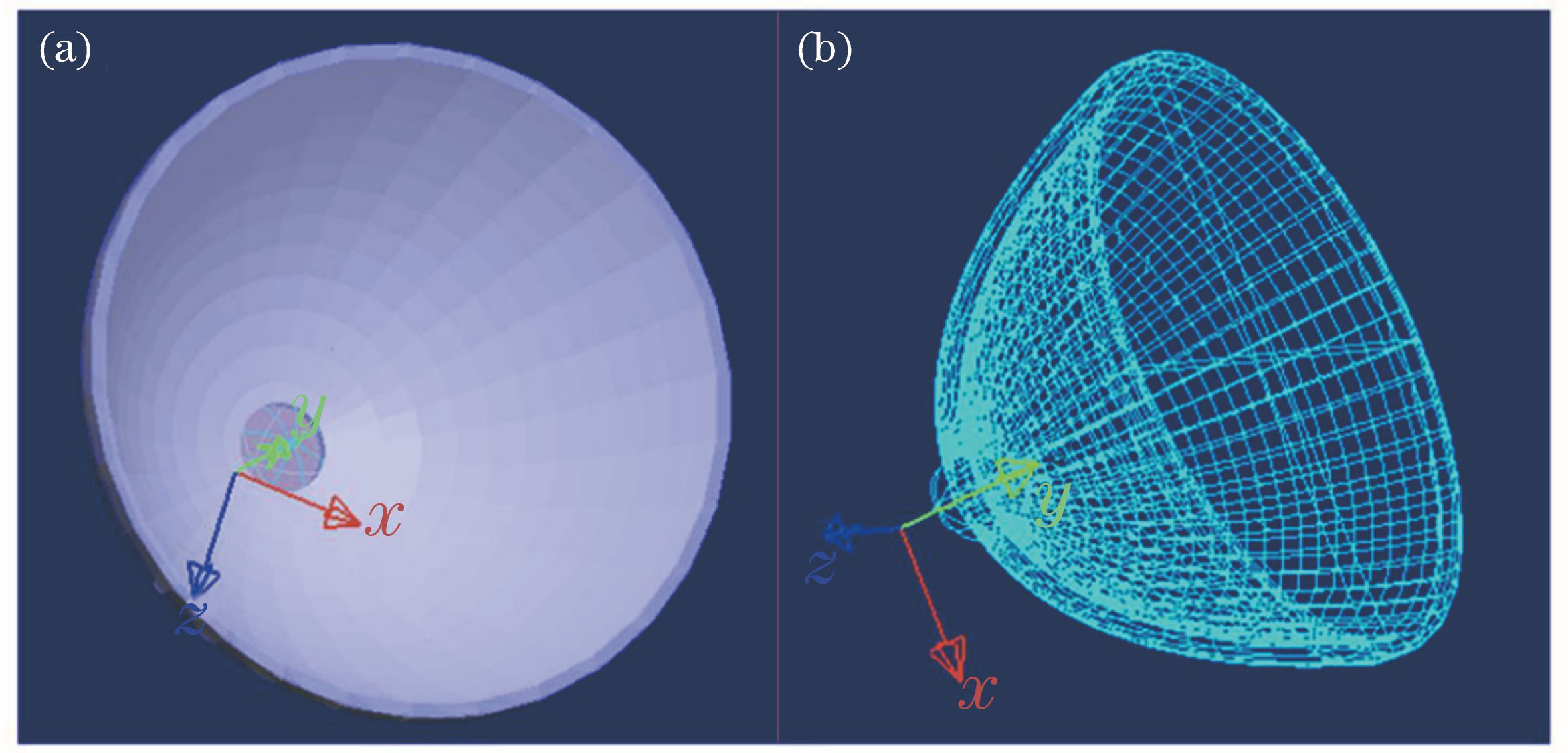
Fig. 1. Outline design of lampshade in LightTools. (a) Fill outline; (b) network cable outline
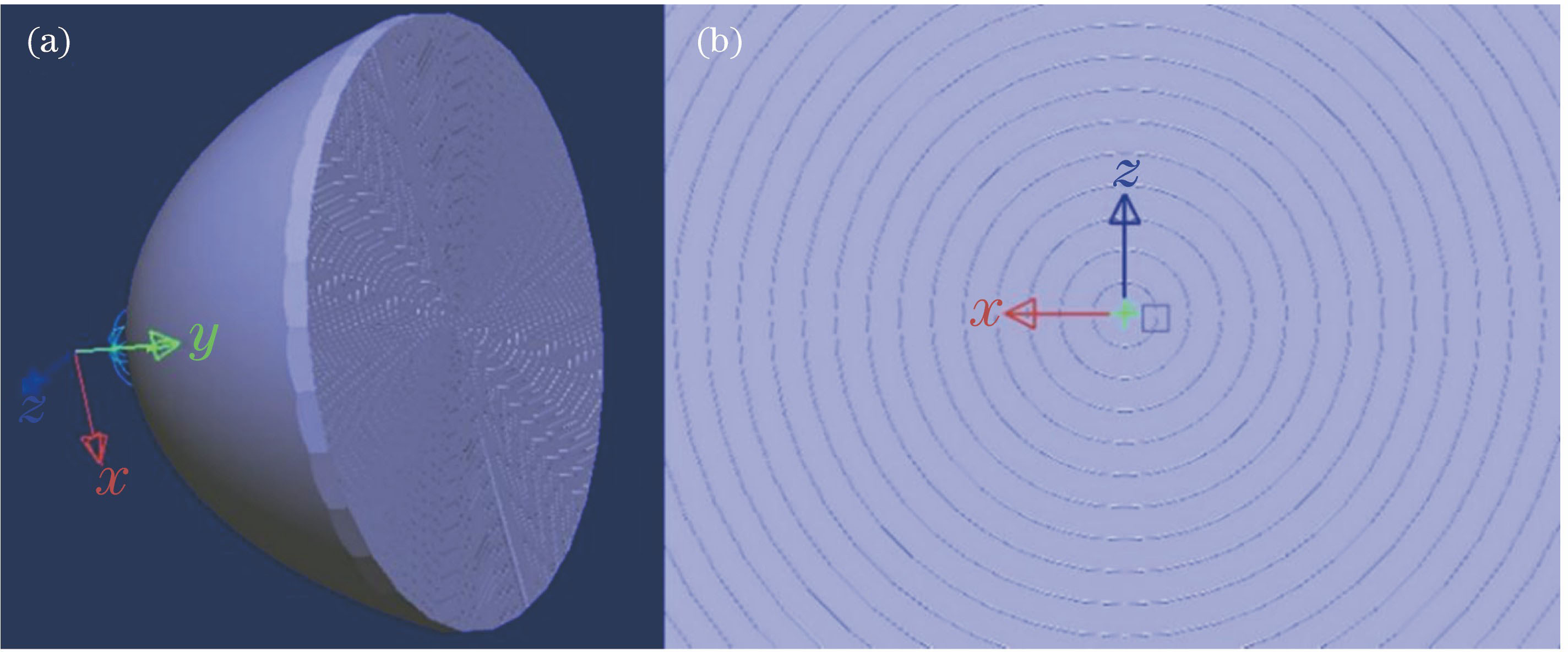
Fig. 2. CD pattern model. (a) Overall model of lampshade; (b) diffuser surface
Fig. 3. Comparison of CD pattern sizes. (a) Center line width is 100 um, and peripheral line width is 200 μm; (b) line width is 300 μm
Fig. 4. Ray tracing simulation of LED downlight lighting system. (a) Ray tracing of single light source; (b) ray tracing with receiver
Fig. 5. Simulation results of ray tracing. (a) Light power density distribution; (b) illumination display curve
Fig. 6. Simulation results of ray tracing at line width of 100 μm. (a) Light power density distribution; (b) illumination display curve
Fig. 7. Simulation results of ray tracing at line width of 200 μm. (a) Light power density distribution; (b) illumination display curve
Fig. 8. Simulation results of ray tracing at a line width of 300 μm. (a) Light power density distribution; (b) illumination display curve
Fig. 9. Injection molding process
Fig. 10. LIGA mold making technology process
Fig. 11. Flow chart of electroforming mold process
Fig. 12. Diagrams of CD pattern microstructure. (a) 3D outline display; (b) 2D flat display
Fig. 13. Diameter test schematic
Fig. 14. Depth test schematic
Fig. 15. Comparison of CD pattern microstructure diffuser and ordinary diffuser. (a) Microstructure diffuser; (b) general diffuser; (c) without diffuser
Fig. 16. Diffusion effect diagrams of light diffusers. (a) CD pattern microstructure diffuser; (b) general diffuser
|
Table 1. Main parameter settings of the model
|
Table 2. Simulation results of LightTools
|
Table 3. Test equipment
|
Table 4. Test data of microstructure diffuser and general diffuser

Set citation alerts for the article
Please enter your email address
© Copyright 2018-2021 | Chinese Laser Press. All Rights Reserved 沪ICP备15018463号-20