
Kaibao Liu, Xiaohong Yang, Tingting He, Hui Wang. Indium Phosphide-Based Near-Infrared Single Photon Avalanche Photodiode Detector Arrays[J]. Laser & Optoelectronics Progress, 2019, 56(22): 220001
- Laser & Optoelectronics Progress
- Vol. 56, Issue 22, 220001 (2019)
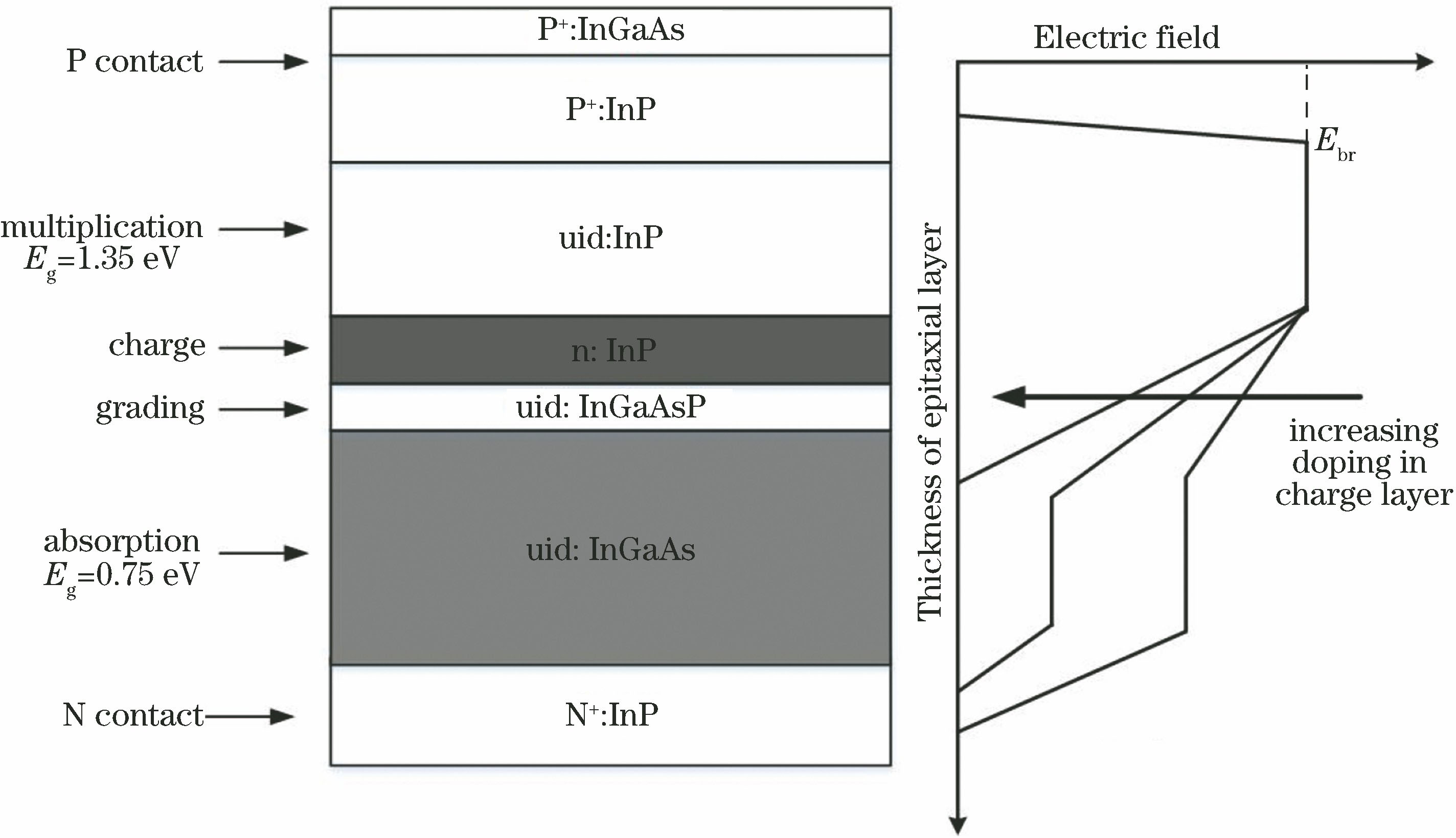
Fig. 1. SAGCM laminated structure and internal electric-field distribution
![Parameter relationships. (a) Relationship between PDE and over-bias at different temperatures[15]; (b) relationship between DCR and PDE for devices with different thicknesses of multiplication layers and fixed PDE[16]](/richHtml/lop/2019/56/22/220001/img_2.jpg)
Fig. 2. Parameter relationships. (a) Relationship between PDE and over-bias at different temperatures[15]; (b) relationship between DCR and PDE for devices with different thicknesses of multiplication layers and fixed PDE[16]
Fig. 3. Parameter relationships. (a) Relationship between DCR and over-bias for devices with different thicknesses of multiplication layers; (b) relationship between DCR and temperature for devices with different thicknesses of multiplication layers at 4 V over-bias[15]
Fig. 4. Device platform design and array image of InGaAsP/InP SPAD. (a) Schematic of epitaxial layer and mesa structure of InGaAsP/InP SPAD designed by MIT; (b) micrograph of individual pixel; (c) micrograph of 4×4 detector array[24]
Fig. 5. APD/CMOS prepared by MIT. (a) Micrograph of bridged 32×32 APD/CMOS array; (b) micrograph of individual pixel in APD/CMOS array at high magnification[26]
Fig. 6. Related parameters and cross-sectional schematic of GM-APD. (a) PDE and crosstalk as functions of over-bias of GM-APD; (b) cross-sectional schematic of InP GM-APD array combined with MLA[33]
Fig. 7. Schematic of focal plane array structure of InP GM-APD. (a) Structure of InGaAs(P)/InP GM-APD; (b) reverse welding GM-APD focal plane array
Fig. 8. 1×16 InGaAs/InP SPAD line array[38]
Fig. 9. Schematic of optical path between two pixels. (a) Without metal trenches; (b) with metal trenches[38]
Fig. 10. InGaAs/InP avalanche photodiode. (a) Schematic of structure; (b) photograph of 8×8 array[39]
|
Table 1. Performance parameters of mesa-type InGaAsP/InP SPAD under different conditions
|
Table 2. Experimental results of array pixel published by Verghese et al.[31] in 2007
|
Table 3. Parameters of focal plane array of InP GM-APD developed by PLI
|
Table 4. DCR and after-pulsing probability statistically distributed at different sizes when PDE is 20% and operating temperature is 233 K
|
Table 5. Comparison of research progresses of various institutions in field of InGaAs/InP SPAD array

Set citation alerts for the article
Please enter your email address
© Copyright 2018-2021 | Chinese Laser Press. All Rights Reserved 沪ICP备15018463号-20