• Photonics Research
  • Vol. 10, Issue 12, 2809 (2022)
A. Pandey, J. Min, Y. Malhotra, M. Reddeppa, Y. Xiao, Y. Wu, and Z. Mi*
Author Affiliations
  • Department of Electrical Engineering and Computer Science, University of Michigan, Ann Arbor, Michigan 48109, USA
  • show less
    DOI: 10.1364/PRJ.473318 Cite this Article Set citation alerts
    A. Pandey, J. Min, Y. Malhotra, M. Reddeppa, Y. Xiao, Y. Wu, Z. Mi. Strain-engineered N-polar InGaN nanowires: towards high-efficiency red LEDs on the micrometer scale[J]. Photonics Research, 2022, 10(12): 2809 Copy Citation Text show less
    (a)–(d) Schematic of selective-area epitaxy of N-polar InGaN/GaN nanowire LED heterostructures. (e) Schematic of a single nanowire LED heterostructure, showing the different layers.
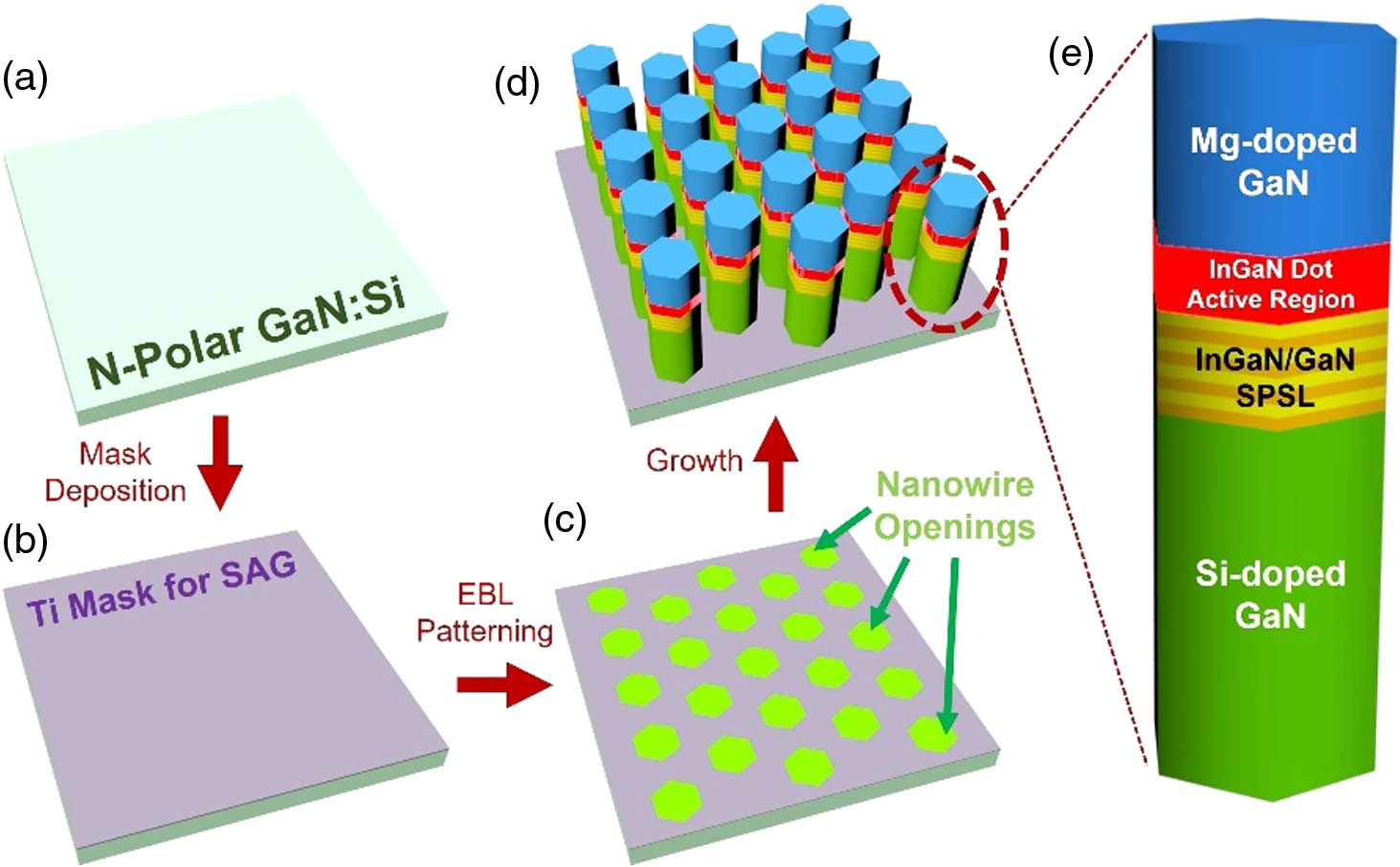
    Fig. 1. (a)–(d) Schematic of selective-area epitaxy of N-polar InGaN/GaN nanowire LED heterostructures. (e) Schematic of a single nanowire LED heterostructure, showing the different layers.
    (a) Scanning electron microscope (SEM) image of an N-polar InGaN/GaN nanowire array. (b) Stacked photoluminescence (PL) spectra of nanowire samples containing only the InGaN/GaN SPSL (green curve), only the InGaN dot active region (orange curve), and both combined (red curve).
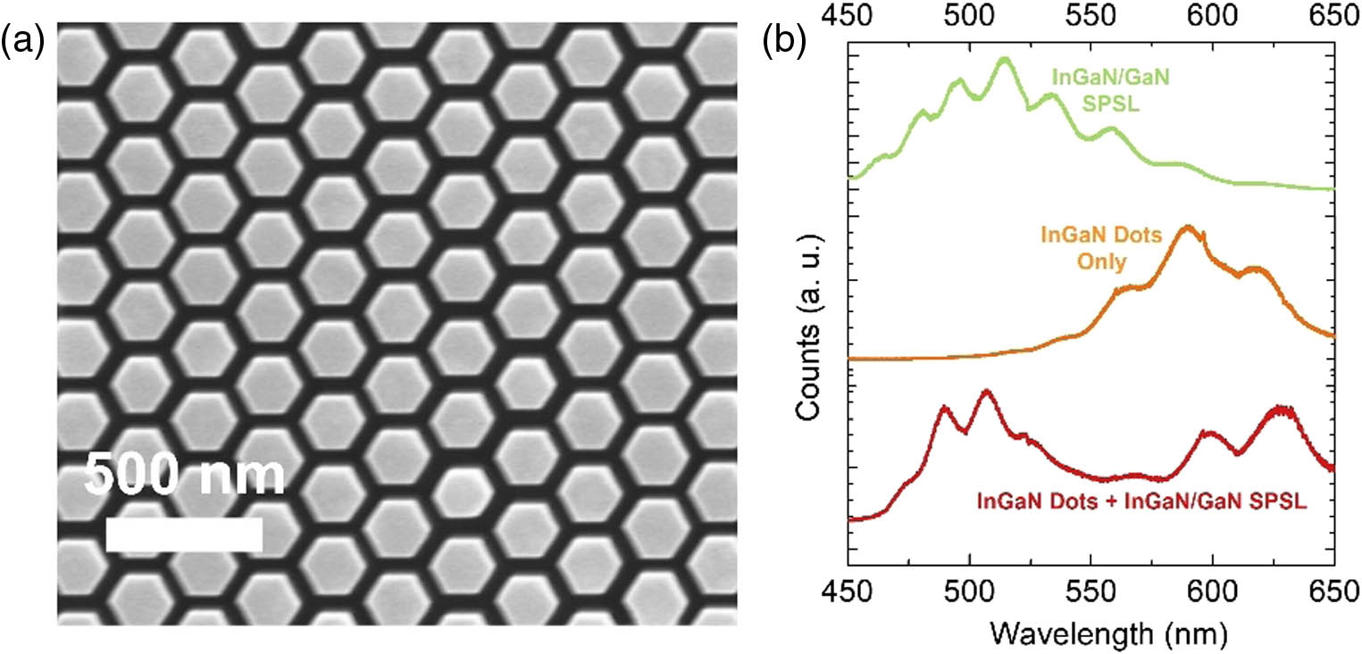
    Fig. 2. (a) Scanning electron microscope (SEM) image of an N-polar InGaN/GaN nanowire array. (b) Stacked photoluminescence (PL) spectra of nanowire samples containing only the InGaN/GaN SPSL (green curve), only the InGaN dot active region (orange curve), and both combined (red curve).
    (a) Simulated J−V characteristics of the nanowire device structure. (b) Energy band diagrams for the device at different injection currents. The different layers are labeled and shaded differently. (c) Plot showing the contribution of luminescence from the InGaN dot and the InGaN SPSL at different injection currents.
    Fig. 3. (a) Simulated JV characteristics of the nanowire device structure. (b) Energy band diagrams for the device at different injection currents. The different layers are labeled and shaded differently. (c) Plot showing the contribution of luminescence from the InGaN dot and the InGaN SPSL at different injection currents.
    (a) Measured J−V characteristics of the sub-micrometer-scale nanowire red microLED. The inset shows an SEM image of a submicrometer device injection opening that has been etched into the SiO2 insulation layer. (b) L−I characteristics of the device. (c) EQE and wall-plug efficiency (WPE) for the device versus injection currents.
    Fig. 4. (a) Measured JV characteristics of the sub-micrometer-scale nanowire red microLED. The inset shows an SEM image of a submicrometer device injection opening that has been etched into the SiO2 insulation layer. (b) LI characteristics of the device. (c) EQE and wall-plug efficiency (WPE) for the device versus injection currents.
    (a) EL spectra measured at low injection currents for a red-emitting microLED device. (b) EL spectra on a logarithmic scale, measured over several orders of magnitude variations in injection currents.
    Fig. 5. (a) EL spectra measured at low injection currents for a red-emitting microLED device. (b) EL spectra on a logarithmic scale, measured over several orders of magnitude variations in injection currents.
    A. Pandey, J. Min, Y. Malhotra, M. Reddeppa, Y. Xiao, Y. Wu, Z. Mi. Strain-engineered N-polar InGaN nanowires: towards high-efficiency red LEDs on the micrometer scale[J]. Photonics Research, 2022, 10(12): 2809
    Download Citation