A. Pandey, J. Min, Y. Malhotra, M. Reddeppa..., Y. Xiao, Y. Wu and Z. Mi*|Show fewer author(s)
Abstract
The absence of efficient red-emitting micrometer-scale light emitting diodes (LEDs), i.e., LEDs with lateral dimensions of 1 μm or less is a major barrier to the adoption of microLEDs in virtual/augmented reality. The underlying challenges include the presence of extensive defects and dislocations for indium-rich InGaN quantum wells, strain-induced quantum-confined Stark effect, and etch-induced surface damage during the fabrication of quantum well microLEDs. Here, we demonstrate a new approach to achieve strong red emission () from dislocation-free N-polar InGaN/GaN nanowires that included an InGaN/GaN short-period superlattice underneath the active region to relax strain and incorporate more indium within the InGaN dot active region. The resulting submicrometer-scale devices show red electroluminescence dominantly from an InGaN dot active region at low-to-moderate injection currents. A peak external quantum efficiency and a wall-plug efficiency of 2.2% and 1.7% were measured, respectively, which, to the best of our knowledge, are the highest values reported for a submicrometer-scale red LED. This study offers a new path to overcome the efficiency bottleneck of red-emitting microLEDs for a broad range of applications including mobile displays, wearable electronics, biomedical sensing, ultrahigh speed optical interconnect, and virtual/augmented reality.1. INTRODUCTION
Microscale light emitting diodes (microLEDs) are the next step in the evolution of LED technology and are projected to show tremendous growth in the next few years as they are incorporated in many emerging applications, such as virtual/augmented reality, ultrahigh resolution mobile displays, wearable electronics, biomedical sensing, and ultrahigh speed optical interconnects. The III nitrides have been established as the dominant material system for visible LED applications, and they are poised to be used as the basis for microLEDs as well. The inherently lower surface recombination velocity of the III nitrides makes them less susceptible, compared to other material systems (e.g., AlGaInP), to nonradiative surface recombination [1,2]. To date, however, the efficiency of microLEDs remains extremely low especially when the lateral size shrinks to a value smaller than a few microns [3,4]. For example, there has been no report of a conventional top–down red-emitting quantum well microLED with external quantum efficiency for a lateral dimension of 1 μm or less to the best of our knowledge. The efficiency bottleneck of microLEDs has been fundamentally limited by structural damage and defects induced by etching during the fabrication of conventional quantum well structures [5,6].
Further, while InGaN-based LEDs have been shown with exceptional efficiencies in the blue wavelength range, their efficiency drops at longer wavelengths, falling to significantly low values for red-emitting devices [4]. For attaining longer emission wavelengths using the InGaN alloy system, a higher amount of In (up to 30%–40%) is required, which is not trivial. Phase separation is commonly seen in InGaN due to the low miscibility of the alloy [7]. Large lattice mismatch between the InGaN active region and the underlying GaN substrate can induce the formation of extensive defects, while also subjecting the InGaN layer to a high compressive strain [8]. The piezoelectric field induced by the strain is a major cause for the quantum-confined Stark effect (QCSE), which reduces radiative recombination efficiency by spatially separating the electron and hole wave functions within typical quantum well active regions [9]. In this regard, various nanoscale engineering approaches have been developed to effectively relax strain in red-emitting LED heterostructures, including the use of porous GaN templates [10–13], V pits [14,15], and nanostructures [16–19]. Red LEDs have also been demonstrated by growing on a 100% biaxially relaxed InGaN/GaN superlattice buffer [20]. The layer was relaxed through the annealing and thermal decomposition of an InGaN underlayer. Tunnel junctions have also been incorporated to improve the carrier injection in red LEDs showing an external quantum efficiency (EQE) of 4.5% for a device size of [21]. Recently, nanowires have been employed to grow dislocation-free nanostructures [22] that cover the entire visible spectrum [23–25] due to the efficient strain relaxation. Moreover, by epitaxially growing nanostructure devices, the plasma etch process used in conventional quantum well LED fabrication can be removed, thereby avoiding damage to the sidewalls of the active region. The sidewalls can be further passivated using atomic layer deposition (ALD) [26,27], which can also fill the gap between nanowires, eliminating a possible route of the formation of leakage paths. Recent studies have further shown the critical advantages of N-polar GaN nanowires in achieving high-efficiency submicrometer-scale LEDs [3,4], including improved hole injection into the active region [28,29] and increased In incorporation as compared to nanostructures grown in the conventional Ga-polar orientation [30].
In this work, we report on a new approach for achieving efficient micrometer-scale red-emitting nanowire LEDs. The N-polar InGaN/GaN nanowire LEDs were grown utilizing plasma-assisted molecular beam epitaxy (MBE) with controlled diameters, spacing, surface morphology, and polarity. To achieve strong red emission () from N-polar InGaN/GaN nanowires, an InGaN/GaN short-period superlattice (SPSL) was incorporated underneath the active region to relax strain and enable the growth of red-emitting InGaN at relatively higher temperatures, thereby reducing the density of point defects and impurities, which generally limit the optical characteristics of In-rich N-polar InGaN [30–33]. A peak external quantum efficiency and a wall-plug efficiency of 2.2% and 1.7% were measured, respectively, for LEDs with a lateral dimension of , which, to the best of our knowledge, are the most efficient submicrometer-scale red LEDs ever reported. We further performed detailed analysis of the charge-carrier transport, injection, and recombination in such strain-engineered red-emitting LEDs, which offers a new path to overcome the efficiency bottleneck of red-emitting microLEDs for a broad range of applications.
Sign up for Photonics Research TOC. Get the latest issue of Photonics Research delivered right to you!Sign up now
2. NANOWIRE EPITAXY AND CHARACTERIZATION
In this paper, N-polar InGaN/GaN nanowire LED heterostructures were grown utilizing the technique of selective area epitaxy. Prior to the nanowire epitaxy, substrates were first prepared by depositing a Ti (10 nm thick) metal mask on a Si-doped N-polar GaN template on a sapphire substrate. Then electron-beam lithography was used to define openings in the Ti mask, which were etched through to expose the GaN substrate using reactive ion etching (RIE). The substrate was then loaded into a Veeco GEN930 plasma-assisted molecular beam epitaxy system for the growth of the nanowires. These steps are schematically shown in Figs. 1(a)–1(d). An thick Si-doped GaN was first grown. The growth rate for this layer was . The growth temperature was then reduced for the growth of the InGaN/GaN SPSL. Previously, superlattices have been used in conjunction with III-nitride nanowires, and they have demonstrated dislocation-free structures with fully elastic strain relaxation [34,35]. To date, however, their applications in microLEDs have not been reported. In this paper, four periods of Si-doped InGaN (9 nm)/GaN (15 nm) superlattices were grown, followed by an in situ annealing in a nitrogen ambient. Such an annealing step as shown previously, can effectively reduce the density of defects [36,37]. The temperature was then ramped down for the growth of the active region, which consists of two InGaN dots, separated by a GaN barrier layer. Previous work has shown that the geometry of InGaN segments within nanowires follows a complicated geometry, with the formation of facets where the InGaN layers grow along the semi-polar planes [34, 38–40]. The InGaN along these facets typically has a higher In content and more strain relaxation, as compared to that in the bulk of the nanowire. The active region was then further annealed, followed by a thin GaN capping layer, after which the temperature was ramped up for the growth of the thick p-type Mg-doped GaN layer. A schematic of the strain-engineered N-polar InGaN/GaN nanowire LED heterostructures is shown in Fig. 1(e).
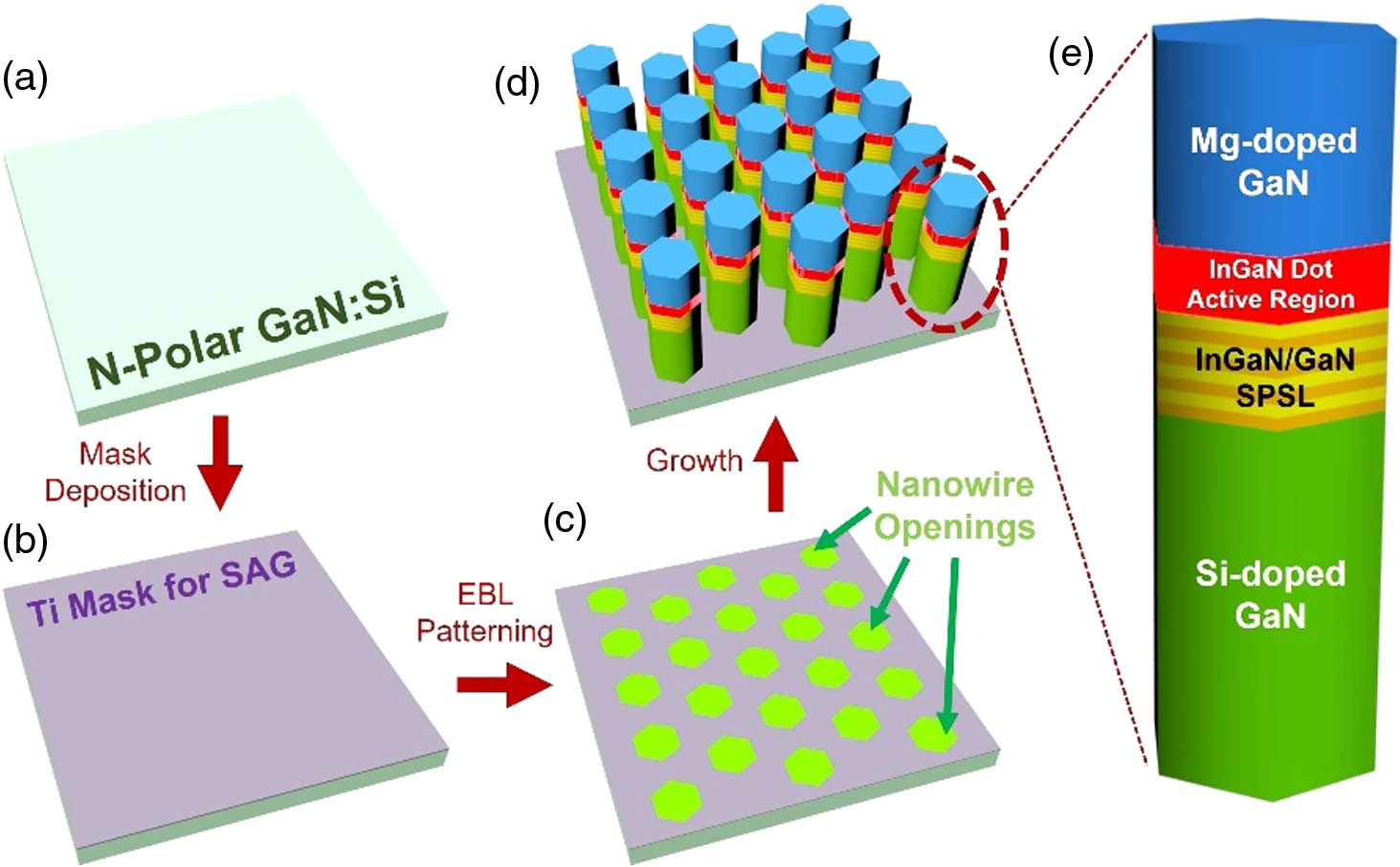
Figure 1.(a)–(d) Schematic of selective-area epitaxy of N-polar InGaN/GaN nanowire LED heterostructures. (e) Schematic of a single nanowire LED heterostructure, showing the different layers.
Shown in Fig. 2(a) is an SEM image of the N-polar nanowire array, which exhibits a uniform morphology and good selectivity. It is seen that such nanowire crystals with precisely controlled diameter, spacing, polarity, and surface morphology, show striking contrasts with previously reported nanowire structures by chemical vapor deposition or by spontaneous formation [25,39,41,42]. The nanowires shown in this image have diameters of with a pitch of . Our previous studies have further shown that such nanowire crystals are free of dislocations due to the efficient strain relaxation [4,43,44]. Optical properties of a strain-engineered N-polar InGaN nanowire heterostructure were studied in detail. For a nanowire sample with the incorporation of only InGaN/GaN SPSL, a distinct emission peaking in the green spectrum is measured, shown in Fig. 2(b) (green curve). On the other hand, for nanowire samples with the incorporation of only InGaN dots (orange curve), the emission is largely limited to the yellow–orange wavelength range. The presence of multiple peaks is due to the optical interference associated with the underlying GaN/sapphire substrate. We have performed extensive growth optimization of the InGaN dot active region. A significant reduction of the PL intensity from the InGaN dots is often measured when the emission peak is shifted to the red spectrum () by further increasing indium incorporation, which is due to the significantly enhanced defect formation in such an indium-rich active region. However, by growing the InGaN dots above the SPSL, we observed a distinct redshift in the emission peak from the dot to 630 nm without any significant degradation of the photoluminescence emission, shown in Fig. 2(b) (red curve). The presence of a strain-engineered InGaN/GaN SPSL can effectively promote strain relaxation within the InGaN dots and enhance indium incorporation, thereby leading to longer wavelength (red) emission. As described previously, these samples were grown with the in situ annealing step as has been previously shown to enhance the intensity of the emission from N-polar InGaN/GaN nanowires [3,4]. It is of note that the red PL emission intensity of the InGaN dots is comparable to that of the green emission from the SPSL, further confirming the effectiveness of such a strain-engineered approach in achieving efficient red emission. The radiative recombination of charge carriers for the microLED device under low-to-moderate electrical injection will primarily occur in the red-emitting InGaN dot active region rather than the green-emitting SPSL due to the low hole mobility and the built-in fields [45,46] to be described next.

Figure 2.(a) Scanning electron microscope (SEM) image of an N-polar InGaN/GaN nanowire array. (b) Stacked photoluminescence (PL) spectra of nanowire samples containing only the InGaN/GaN SPSL (green curve), only the InGaN dot active region (orange curve), and both combined (red curve).
3. DEVICE SIMULATIONS
The device structure described was further simulated using Silvaco Atlas with standard parameters [29]. In this study, the presence of surface recombination is not considered, and the polarization field in the InGaN layers within the superlattice and active region is assumed to be 25% of the theoretical value, considering the effects of the thick layers and polarization field screening [47,48]. The simulated characteristics are shown in Fig. 3(a). The relatively high turn-on voltage is due to the use of a relatively thick active region and the low doping assumed in the superlattice layers. The band diagrams at equilibrium, at a low injection current of , and a moderate injection current of are calculated and plotted in Fig. 3(b). These diagrams show a small barrier to hole injection into the first dot from the p-GaN layer at equilibrium, while, at low injection this barrier almost disappears. At higher injections, it is possible to inject holes into the superlattice layer as well, resulting in luminescence emission from that layer. The relative ratio of radiative recombination within the InGaN dot active region and the superlattice is further simulated and plotted in Fig. 3(c). At lower injection currents, the emission is confined to the InGaN dot active region with almost all of the emission originating in the active region. As the current increases, the emission from the superlattice layers starts to increase, and it becomes non-negligible for currents at and above . It is also of note that recently reported high-efficiency N-polar nanowire-based LEDs show a peak in EQE at relatively low injection currents () [3,4], which also corresponds to the regime where we see emission primarily from the red-emitting InGaN dot active region. For applications in the emerging virtual reality, high efficiency, ultralow power, and ultrasmall size LEDs are essentially required. In this regard, the presented design is well suited for such applications. Moreover, the design of the InGaN SPSL and dot active region can be further optimized to achieve predominantly red emission at even higher current densities.
Figure 3.(a) Simulated characteristics of the nanowire device structure. (b) Energy band diagrams for the device at different injection currents. The different layers are labeled and shaded differently. (c) Plot showing the contribution of luminescence from the InGaN dot and the InGaN SPSL at different injection currents.
4. DEVICE FABRICATION AND MEASUREMENTS
To fabricate nanowire microLED devices, the gaps in between the wires were first filled using ALD of . The on the top of the nanowires was carefully etched using RIE to expose the top p-GaN layer of the nanowires. This was followed by a plasma-enhanced chemical vapor deposition of to act as the insulation layer into which submicrometer vias were defined by projection lithography. The injection window had a diameter of , defining the area of the microLED. The in these openings was etched using RIE until the nanowires were visible. An SEM image of one such etched device opening, having nanowires with diameters of and pitch of , is shown in the inset of Fig. 4(a). Ti/Au (20 nm/100 nm) metal contacts were then deposited for the n contact, while, Ni/Au/ITO (5 nm/5 nm/200 nm) was deposited for the p contact. The devices were then annealed in a forming gas ambient. Finally, a reflective Ag/Ti/Al/Ni/Au (100 nm/20 nm/100 nm/20 nm/50 nm) contact pad was deposited over the devices to facilitate light collection from the back of the wafer.
Figure 4.(a) Measured characteristics of the sub-micrometer-scale nanowire red microLED. The inset shows an SEM image of a submicrometer device injection opening that has been etched into the insulation layer. (b) characteristics of the device. (c) EQE and wall-plug efficiency (WPE) for the device versus injection currents.
Figure 4(a) shows the characteristics of a fabricated device having a nanowire diameter of and a pitch of 360 nm. The devices show negligible leakage current under reverse bias with excellent rectification. In forward bias, the devices show a turn-on at . To measure the output power of the device, we placed it directly on a Newport 918D-ST-UV detector and collected the power on-wafer from the back of the sapphire substrate. The characteristics of the device are shown in Fig. 4(b). It is seen that the output power increases with injection current. However, a noticeable change in the slope is observed around , which corresponds approximately to the transition from dominantly red emission to green emission (to be described next), in good agreement with the simulation shown in Fig. 3(c). The corresponding EQE and WPE plots for the device are shown in Fig. 4(c). A peak EQE of and a WPE of were achieved at a current density of . To the best of our knowledge, this is the highest EQE reported for a red-emitting () micro-LED with lateral dimensions on the order of 1 μm or less. It is also noted that there is a significant efficiency droop, which can be minimized by further optimizing the design and by incorporating an AlGaN electron blocking layer.
We also studied the variation of the electroluminescence (EL) with injection current. Shown in Fig. 5(a) is a plot of the EL spectra for the device measured at different injection currents. At low injection currents of around and less, the emission peaks at , putting it in the red region of the visible spectrum. However, as the injection current increases, the emission at starts to dominate the spectrum, making the emission appear more orange/amber. The peak at is related to parasitic emission from the SPSL in this sample, whereas the longer wavelength emission at originates from the InGaN dot active region. When the injection current is increased even further, shown in Fig. 5(b), the SPSL emission becomes the primary peak, making the device emission appear yellow. The emission from the dots appears as a shoulder at at high injection currents, and the position of this emission does not show much change with injection current. This is likely due to the efficient strain relaxation in the active region induced by the growth of the SPSL. The reduced strain in the active region minimizes the effect of the QCSE, allowing for stable emission.
Figure 5.(a) EL spectra measured at low injection currents for a red-emitting microLED device. (b) EL spectra on a logarithmic scale, measured over several orders of magnitude variations in injection currents.
5. CONCLUSIONS
Previously, the use of thick InGaN and superlattice structures underlying an InGaN-based active region has been demonstrated to release strain within the active region, resulting in redshifted emission wavelengths for conventional quantum well LEDs [20,49–52]. However, within conventional planar LED heterostructures, a relatively thick buffer or a superlattice layer must be utilized in order to effectively relax strain, and the relative mismatch between the layers needs to be minimized to prevent the generation of extensive defects [53,54], thereby preventing the realization of efficient red LEDs. For planar structures, the use of thermal annealing has been shown to effectively relax InGaN buffer layers, however, the surface morphology was characterized by large pits. As such, red LEDs demonstrated using these processes showed very low efficiencies [20]. These issues can be fundamentally addressed in bottom–up nanostructures, allowing for extremely effective strain relaxation even with a thin superlattice stack, making it much easier to attain red emission as we have shown here. As this technique relied only on epitaxy, it avoided regrowth and extra processing steps that can be difficult to control in other methods, such as making the substrate porous. It also retains the advantages of nanowire processing, namely, the avoidance of a mesa etch step during the fabrication of microLEDs. These factors have contributed to the demonstration of a red-emitting submicrometer-scale LED with an external quantum efficiency for the first time.
To summarize, we have incorporated an InGaN/GaN SPSL into a red-emitting N-polar nanowire heterostructure to achieve red emission. With this unique design, we demonstrated submicrometer-scale LEDs with emissions at and peak EQEs of 2.2% for an unpackaged device. The EL of the devices showed a negligible change in the emission wavelength of the InGaN active region peak with increasing injection current because of the efficient strain relaxation in the active region which inhibited QCSE. The issues of spectral purity and extraneous emissions at higher currents can be minimized through improvements in the design of the LED heterostructure devices, which can effectively limit recombination to the active region. This shows the promise of the nanowire-based approach for high-efficiency microLEDs.
Acknowledgment
Acknowledgment. The authors wish to thank S. Yang for discussions and development of the Silvaco model.
References
[1] M. Boroditsky, I. Gontijo, M. Jackson, R. Vrijen, E. Yablonovitch, T. Krauss, C.-C. Cheng, A. Scherer, R. Bhat, M. Krames. Surface recombination measurements on III–V candidate materials for nanostructure light-emitting diodes. J. Appl. Phys., 87, 3497-3504(2000).
[2] J. M. Smith, R. Ley, M. S. Wong, Y. H. Baek, J. H. Kang, C. H. Kim, M. J. Gordon, S. Nakamura, J. S. Speck, S. P. DenBaars. Comparison of size-dependent characteristics of blue and green InGaN microLEDs down to 1 μm in diameter. Appl. Phys. Lett., 116, 071102(2020).
[3] A. Pandey, Y. Malhotra, P. Wang, K. Sun, X. Liu, Z. Mi. N-polar InGaN/GaN nanowires: overcoming the efficiency cliff of red-emitting micro-LEDs. Photon. Res., 10, 1107-1116(2022).
[4] X. Liu, Y. Sun, Y. Malhotra, A. Pandey, P. Wang, Y. Wu, K. Sun, Z. Mi. N-polar InGaN nanowires: breaking the efficiency bottleneck of nano and micro LEDs. Photon. Res., 10, 587-593(2022).
[5] M. Minami, S. Tomiya, K. Ishikawa, R. Matsumoto, S. Chen, M. Fukasawa, F. Uesawa, M. Sekine, M. Hori, T. Tatsumi. Analysis of GaN damage induced by Cl2/SiCl4/Ar plasma. Jpn. J. Appl. Phys., 50, 08JE03(2011).
[6] Y. B. Hahn, R. J. Choi, J. H. Hong, H. J. Park, C. S. Choi, H. J. Lee. High-density plasma-induced etch damage of InGaN/GaN multiple quantum well light-emitting diodes. J. Appl. Phys., 92, 1189-1194(2002).
[7] I. Ho, G. B. Stringfellow. Solid phase immiscibility in GaInN. Appl. Phys. Lett., 69, 2701-2703(1996).
[8] T. Langer, A. Kruse, F. A. Ketzer, A. Schwiegel, L. Hoffmann, H. Jönen, H. Bremers, U. Rossow, A. Hangleiter. Origin of the ‘green gap’: increasing nonradiative recombination in indium-rich GaInN/GaN quantum well structures. Phys. Status Solidi C, 8, 2170-2172(2011).
[9] T. Takeuchi, S. Sota, M. Katsuragawa, M. Komori, H. Takeuchi, H. A. H. Amano, I. A. I. Akasaki. Quantum-confined Stark effect due to piezoelectric fields in GaInN strained quantum wells. Jpn. J. Appl. Phys., 36, L382(1997).
[10] S. S. Pasayat, C. Gupta, M. S. Wong, Y. Wang, S. Nakamura, S. P. Denbaars, S. Keller, U. K. Mishra. Growth of strain-relaxed InGaN on micrometer-sized patterned compliant GaN pseudo-substrates. Appl. Phys. Lett., 116, 111101(2020).
[11] S. S. Pasayat, R. Ley, C. Gupta, M. S. Wong, C. Lynsky, Y. Wang, M. J. Gordon, S. Nakamura, S. P. Denbaars, S. Keller, U. K. Mishra. Color-tunable <10 μm square InGaN micro-LEDs on compliant GaN-on-porous-GaN pseudo-substrates. Appl. Phys. Lett., 117, 061105(2020).
[12] S. Keller, S. S. Pasayat, C. Gupta, S. P. DenBaars, S. Nakamura, U. K. Mishra. Patterned III-nitrides on porous GaN: extending elastic relaxation from the nano- to the micrometer scale. Phys. Status Solidi (RRL), 15, 2100234(2021).
[13] S. S. Pasayat, C. Gupta, M. S. Wong, R. Ley, M. J. Gordon, S. P. DenBaars, S. Nakamura, S. Keller, U. K. Mishra. Demonstration of ultra-small (<10 μm) 632 nm red InGaN micro-LEDs with useful on-wafer external quantum efficiency (>0.2%) for mini-displays. Appl. Phys. Express, 14, 011004(2020).
[14] S. Zhang, J. Zhang, J. Gao, X. Wang, C. Zheng, M. Zhang, X. Wu, L. Xu, J. Ding, Z. Quan, F. Jiang. Efficient emission of InGaN-based light-emitting diodes: toward orange and red. Photonics Res., 8, 1671-1675(2020).
[15] W. Yao, L. Wang, Y. Meng, S. Yang, X. Liu, H. Niu, Z. Wang. Stress engineering for reducing the injection current induced blue shift in InGaN-based red light-emitting diodes. CrystEngComm, 23, 2360-2366(2021).
[16] R. Vadivelu, Y. Igawa, K. Kishino. 633 nm red emissions from InGaN nanocolumn light-emitting diode by radio frequency plasma assisted molecular beam epitaxy. Jpn. J. Appl. Phys., 52, 08JE18(2013).
[17] P. Feng, C. Xu, J. Bai, C. Zhu, I. Farrer, G. Martinez de Arriba, T. Wang. A simple approach to achieving ultrasmall III-nitride microlight-emitting diodes with red emission. ACS Appl. Electron. Mater., 4, 2787-2792(2022).
[18] B. Jenichen, O. Brandt, C. Pfüller, P. Dogan, M. Knelangen, A. Trampert. Macro-and micro-strain in GaN nanowires on Si (111). Nanotechnol., 22, 295714(2011).
[19] F. Glas. Critical dimensions for the plastic relaxation of strained axial heterostructures in free-standing nanowires. Phys. Rev. B, 74, 121302(2006).
[20] P. Chan, V. Rienzi, N. Lim, H.-M. Chang, M. Gordon, S. P. DenBaars, S. Nakamura. Demonstration of relaxed InGaN-based red LEDs grown with high active region temperature. Appl. Phys. Express, 14, 101002(2021).
[21] P. Li, H. Li, H. Zhang, Y. Yang, M. S. Wong, C. Lynsky, M. Iza, M. J. Gordon, J. S. Speck, S. Nakamura, S. P. DenBaars. Red InGaN micro-light-emitting diodes (> 620 nm) with a peak external quantum efficiency of 4.5% using an epitaxial tunnel junction contact. Appl. Phys. Lett., 120, 121102(2022).
[22] K. Kishino, S. Ishizawa. Selective-area growth of GaN nanocolumns on Si (111) substrates for application to nanocolumn emitters with systematic analysis of dislocation filtering effect of nanocolumns. Nanotechnol., 26, 225602(2015).
[23] S. Jahangir, M. Mandl, M. Strassburg, P. Bhattacharya. Molecular beam epitaxial growth and optical properties of red-emitting (λ = 650 nm) InGaN/GaN disks-in-nanowires on silicon. Appl. Phys. Lett., 102, 071101(2013).
[24] A. Kikuchi, M. Tada, K. Miwa, K. Kishino. Growth and characterization of InGaN/GaN nanocolumn LED. Proc. SPIE, 6129, 612905(2006).
[25] W. Guo, M. Zhang, A. Banerjee, P. Bhattacharya. Catalyst-free InGaN/GaN nanowire light emitting diodes grown on (001) silicon by molecular beam epitaxy. Nano Lett., 10, 3355-3359(2010).
[26] D.-H. Lee, J.-H. Lee, J.-S. Park, T.-Y. Seong, H. Amano. Improving the leakage characteristics and efficiency of GaN-based micro-light-emitting diode with optimized passivation. ECS J. Solid State Sci. Technol., 9, 055001(2020).
[27] M. Latzel, P. Büttner, G. Sarau, K. Höflich, M. Heilmann, W. Chen, X. Wen, G. Conibeer, S. H. Christiansen. Significant performance enhancement of InGaN/GaN nanorod LEDs with multi-layer graphene transparent electrodes by alumina surface passivation. Nanotechnol., 28, 055201(2016).
[28] G. Deng, Y. Zhang, Y. Yu, L. Yan, P. Li, X. Han, L. Chen, D. Zhao, G. Du. Simulation and fabrication of N-polar GaN-based blue-green light-emitting diodes with p-type AlGaN electron blocking layer. J. Mater. Sci.: Mater. Electron., 29, 9321-9325(2018).
[29] F. Akyol, D. N. Nath, S. Krishnamoorthy, P. S. Park, S. Rajan. Suppression of electron overflow and efficiency droop in N-polar GaN green light emitting diodes. Appl. Phys. Lett., 100, 111118(2012).
[30] S. Keller, N. A. Fichtenbaum, M. Furukawa, J. S. Speck, S. P. DenBaars, U. K. Mishra. Growth and characterization of N-polar InGaN/GaN multiquantum wells. Appl. Phys. Lett., 90, 191908(2007).
[31] D. N. Nath, E. Gür, S. A. Ringel, S. Rajan. Molecular beam epitaxy of N-polar InGaN. Appl. Phys. Lett., 97, 071903(2010).
[32] F. Tuomisto, K. Saarinen, B. Lucznik, I. Grzegory, H. Teisseyre, T. Suski, S. Porowski, P. R. Hageman, J. Likonen. Effect of growth polarity on vacancy defect and impurity incorporation in dislocation-free GaN. Appl. Phys. Lett., 86, 031915(2005).
[33] C. Chéze, M. Siekacz, G. Muzioł, H. Turski, S. Grzanka, M. Kryśko, J. L. Weyher, M. Boćkowski, C. Hauswald, J. Lähnemann, O. Brandt, M. Albrecht, C. Skierbiszewski. Investigation on the origin of luminescence quenching in N-polar (In,Ga)N multiple quantum wells. J. Vac. Sci. Technol. B, 31, 03C130(2013).
[34] T. Kehagias, G. Dimitrakopulos, P. Becker, J. Kioseoglou, F. Furtmayr, T. Koukoula, I. Häusler, A. Chernikov, S. Chatterjee, T. Karakostas. Nanostructure and strain in InGaN/GaN superlattices grown in GaN nanowires. Nanotechnol., 24, 435702(2013).
[35] O. Landré, D. Camacho, C. Bougerol, Y.-M. Niquet, V. Favre-Nicolin, G. Renaud, H. Renevier, B. Daudin. Elastic strain relaxation in GaN/AlN nanowire superlattice. Phys. Rev. B, 81, 153306(2010).
[36] N. A. K. Kaufmann, A. Dussaigne, D. Martin, P. Valvin, T. Guillet, B. Gil, F. Ivaldi, S. Kret, N. Grandjean. Thermal annealing of molecular beam epitaxy-grown InGaN/GaN single quantum well. Semicond. Sci. Technol., 27, 105023(2012).
[37] X. Zhang, H. Lourenço-Martins, S. Meuret, M. Kociak, B. Haas, J.-L. Rouvière, P.-H. Jouneau, C. Bougerol, T. Auzelle, D. Jalabert, X. Biquard, B. Gayral, B. Daudin. InGaN nanowires with high InN molar fraction: growth, structural and optical properties. Nanotechnol., 27, 195704(2016).
[38] C. Zhao, T. K. Ng, N. Wei, A. Prabaswara, M. S. Alias, B. Janjua, C. Shen, B. S. Ooi. Facile formation of high-quality InGaN/GaN quantum-disks-in-nanowires on bulk-metal substrates for high-power light-emitters. Nano Lett., 16, 1056-1063(2016).
[39] G. Tourbot, C. Bougerol, F. Glas, L. F. Zagonel, Z. Mahfoud, S. Meuret, P. Gilet, M. Kociak, B. Gayral, B. Daudin. Growth mechanism and properties of InGaN insertions in GaN nanowires. Nanotechnol., 23, 135703(2012).
[40] B. Park, J. K. Lee, C. T. Koch, M. Wölz, L. Geelhaar, S. H. Oh. High‐resolution mapping of strain partitioning and relaxation in InGaN/GaN nanowire heterostructures. Adv. Sci., 9, 2200323(2022).
[41] H. C. Kuo, T. S. Oh, P.-C. Ku. MOCVD growth of vertically aligned InGaN nanowires. J. Cryst. Growth, 370, 311-313(2013).
[42] Y.-H. Ra, R. Navamathavan, C.-R. Lee. Growth characteristics of uniaxial InGaN/GaN MQW/n-GaN nanowires on Si (111) using MOCVD. CrystEngComm, 14, 8208-8214(2012).
[43] H. P. T. Nguyen, K. Cui, S. Zhang, M. Djavid, A. Korinek, G. A. Botton, Z. Mi. Controlling electron overflow in phosphor-free InGaN/GaN nanowire white light-emitting diodes. Nano Lett., 12, 1317-1323(2012).
[44] B. H. Le, S. Zhao, X. Liu, S. Y. Woo, G. A. Botton, Z. Mi. Controlled coalescence of AlGaN nanowire arrays: an architecture for nearly dislocation-free planar ultraviolet photonic device applications. Adv. Mater., 28, 8446-8454(2016).
[45] Y.-K. Kuo, Y.-A. Chang. Effects of electronic current overflow and inhomogeneous carrier distribution on InGaN quantum-well laser performance. IEEE J. Quantum Electron., 40, 437-444(2004).
[46] R. Charash, P. P. Maaskant, L. Lewis, C. McAleese, M. J. Kappers, C. J. Humphreys, B. Corbett. Carrier distribution in InGaN/GaN tricolor multiple quantum well light emitting diodes. Appl. Phys. Lett., 95, 151103(2009).
[47] V. Fiorentini, F. Bernardini, F. Della Sala, A. Di Carlo, P. Lugli. Effects of macroscopic polarization in III-V nitride multiple quantum wells. Phys. Rev. B, 60, 8849-8858(1999).
[48] O. Mayrock, H.-J. Wünsche, F. Henneberger. Polarization charge screening and indium surface segregation in (In,Ga)N/GaN single and multiple quantum wells. Phys. Rev. B, 62, 16870-16880(2000).
[49] J. Zhang, N. Tansu. Improvement in spontaneous emission rates for InGaN quantum wells on ternary InGaN substrate for light-emitting diodes. J. Appl. Phys., 110, 113110(2011).
[50] A. Dussaigne, F. Barbier, B. Samuel, A. Even, R. Templier, F. Lévy, O. Ledoux, M. Rozhavskaia, D. Sotta. Strongly reduced V pit density on InGaNOS substrate by using InGaN/GaN superlattice. J. Cryst. Growth, 533, 125481(2020).
[51] J. Däubler, T. Passow, R. Aidam, K. Köhler, L. Kirste, M. Kunzer, J. Wagner. Long wavelength emitting GaInN quantum wells on metamorphic GaInN buffer layers with enlarged in-plane lattice parameter. Appl. Phys. Lett., 105, 111111(2014).
[52] K. Hestroffer, F. Wu, H. Li, C. Lund, S. Keller, J. S. Speck, U. K. Mishra. Relaxed c-plane InGaN layers for the growth of strain-reduced InGaN quantum wells. Semicond. Sci. Technol., 30, 105015(2015).
[53] W. Li, P. Bergman, I. Ivanov, W.-X. Ni, H. Amano, I. Akasa. High-resolution X-ray analysis of InGaN/GaN superlattices grown on sapphire substrates with GaN layers. Appl. Phys. Lett., 69, 3390-3392(1996).
[54] S. J. Leem, Y. C. Shin, K. C. Kim, E. H. Kim, Y. M. Sung, Y. Moon, S. M. Hwang, T. G. Kim. The effect of the low-mole InGaN structure and InGaN/GaN strained layer superlattices on optical performance of multiple quantum well active layers. J. Cryst. Growth, 311, 103-106(2008).


