
Tianxun Gong, Boyuan Yan, Taiping Zhang, Wen Huang, Yuhao He, Xiaoyu Xu, Song Sun, Xiaosheng Zhang. Fano resonance-enhanced Si/MoS2 photodetector[J]. Photonics Research, 2023, 11(12): 2159
- Photonics Research
- Vol. 11, Issue 12, 2159 (2023)
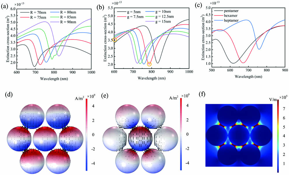
Fig. 1. (a) Effect of changing nanoparticle size on the Fano resonance dip position. (b) Effect of changing nanoparticle spacing on the Fano resonance dip position. (c) Effect of changing the number of particles (heptamer, hexamer, and pentamer) on the Fano resonance dip position. (d) Surface current density and displacement current distribution (arrows) at 600 nm. (e) Surface current density and displacement current distribution (arrows) at the Fano dip wavelength (785 nm). (f) Calculated normalized electric field distribution of the heptamer structure.
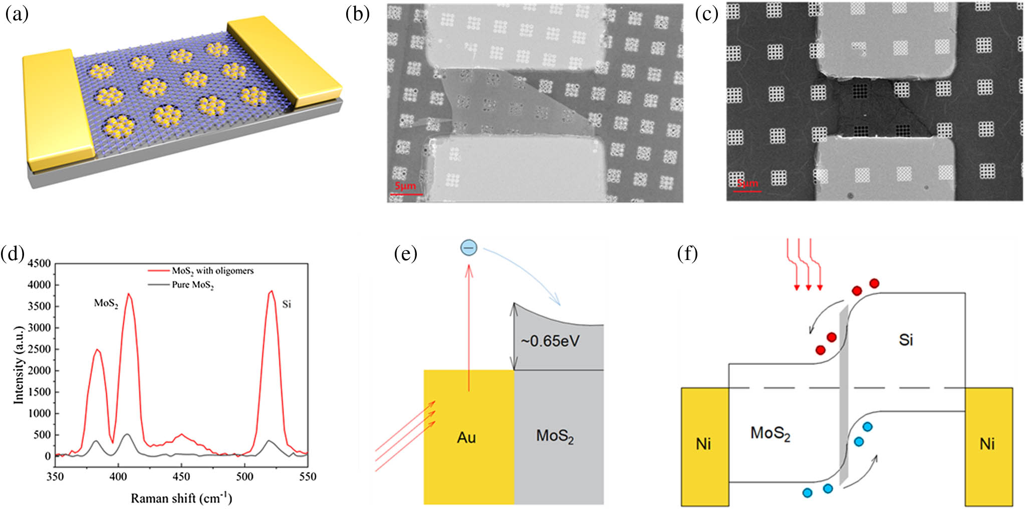
Fig. 2. (a) Schematic of the photodetector. (b) SEM image of the photodetector. (c) SEM images of the photodetectors of the control group. (d) Raman spectra of the MoS 2 Au - MoS 2 Si / MoS 2
Fig. 3. I-V characteristic curves of devices at (a) 450 nm, (b) 520 nm, (c) 635 nm, (d) 785 nm, and (e) 1064 nm, respectively.
Fig. 4. (a) Responsivity and detectivity of the device at different optical powers. (b) I-T response of the proposed device. (c) Comparison of the responsivity of the device and the control.
Fig. 5. (a) Heptamer structure. R is the radius of AuNPs, and g is the distance between the central nanoparticles and the surrounding nanoparticles. (b) Schematic diagram of the hexamer. (c) Schematic diagram of the pentamer.
Fig. 6. (a) Schematic view of the silicon substrate with a hole array. (b) Silicon substrate with oligomer structures. (c) Substrate with a few layers of MoS 2 MoS 2
Fig. 7. (a) SEM picture of the fabricated nanohole array. (b) Side view of the nanohole.
Fig. 8. (a) Schematic of the CAPA method. (b)–(d) SEM images of the CAPA effect.
Fig. 9. SEM images of the oligomers on hole array substrate.
Fig. 10. Reflectance spectrum of the oligomers on the hole array substrate.
|
Table 1. Performance Comparison of Photodetector-Based MoS2

Set citation alerts for the article
Please enter your email address
© Copyright 2018-2021 | Chinese Laser Press. All Rights Reserved 沪ICP备15018463号-20