1School of Integrated Circuit Science and Engineering (Exemplary School of Microelectronics), University of Electronic Science and Technology of China, Chengdu 611731, China
2Tianfu Xinglong Lake Laboratory, Chengdu 610299, China
3Microsystem and Terahertz Research Center, China Academy of Engineering Physics, Chengdu 610200, China
4Institute of Electronic Engineering, China Academy of Engineering Physics, Mianyang 621900, China
In this work, a heterojunction photodetector enhanced by hot electron injection through Fano resonance is developed. By preparing Au oligomers using capillary-assisted particle assembly (CAPA) on the silicon substrate with a nanohole array and covering few-layer with Au electrodes on top of the oligomer structures, the Fano resonance couples with a heterojunction. With on-resonance excitation, Fano resonance generated many hot electrons on the surface of oligomers, and the hot electrons were injected into , providing an increased current in the photodetector under a bias voltage. The photodetectors exhibited a broadband photoresponse ranging from 450 to 1064 nm, and a large responsivity up to 52 A/W at a wavelength of 785 nm under a bias voltage of 3 V. The demonstrated Fano resonance-enhanced heterojunction photodetector provides a strategy to improve the photoresponsivity of two-dimensional materials-based photodetectors for optoelectronic applications in the field of visible and near-infrared detection.
1. INTRODUCTION
As a typical transition metal disulphide, has a band gap ranging from an indirect bandgap (1.2 eV) to a single-layer direct bandgap (1.9 eV) [1,2], which brings about broadband light absorption capacity and medium carrier mobility [3–5]. Based on these characteristics, has been studied and applied in many fields, such as phototransistor [6–8], solar cell [9–11], and photodetector [12–15]. Nevertheless, the light absorption capacity of few-layer or single-layer is relatively weak [14,16], resulting in unsatisfactory photocurrent generation.
To improve the optical absorption in , many methods have been proposed, such as adopting heterostructures [17–24], photonic crystals [25,26], and transistors [27]. One promising strategy is to integrate with noble metal nanoparticles and couple the surface plasmon resonance (SPR) with through hot electron injection to enhance the light absorption [28,29]. However, most of the noble nanoparticles in such devices are drop-coated, which leads to uneven signal enhancement. Furthermore, the conventional surface plasmon resonance produced in such devices has a weak optical resonance and large radiation loss; thus, the enhancement effect is limited [30].
Here, we proposed a method to enhance the light absorption of in the visible and near-infrared regime using Fano resonance. In particular, Fano resonances originated from the interference between light directly coupled to a bright mode (continuum), and light indirectly coupled to a dark mode (subradiant) excited via near-field interactions with the bright mode [31,32]. The bright mode is associated with optical scattering, while the dark mode preferentially traps the light energy and therefore suppresses scattering. As a result, a Fano resonance is typically characterized as a narrowband dip embedded within a broadband peak in the scattering spectrum [33]. The dark mode of Fano resonance corresponds to strong near-field trapping and enhanced absorption of light energy compared to conventional SPR [33–35]. To fabricate the Fano resonance structure, the capillary-assisted particle assembly (CAPA) method is used to assemble the oligomer of gold nanoparticles (AuNPs) on the silicon substrate with a uniform nanohole array (Appendix B). As the diameter of the nanohole is fixed to , with the spatial limitation, heptamers, hexamers, and pentamers can be formed by using AuNPs each with a diameter of 160 nm. A few layers of were transferred above the oligomer structures and formeda heterojunction with the underlying silicon wafer (Fig. 6 in Appendix B). The oligomers can generate strong Fano resonance from to 830 nm, and the light absorption of is enhanced through the hot electron ejection from the Fano resonance generated by the oligomer structures. The proposed photodetector exhibits a broadband photoresponse ranging from 450 to 1064 nm and a large responsivity up to 52 A/W under 3 V bias voltage at 785 nm light illumination, which is four times higher than that of a photodetector without Fano resonance enhancement.
Sign up for Photonics Research TOC. Get the latest issue of Photonics Research delivered right to you!Sign up now
2. EXPERIMENT
A. Material Sources
The dispersion of gold nanoparticles is directly purchased from Biotyscience (ABNW-1-160). The few-layer is prepared through mechanical exfoliation from bulk (SixCarbon Technology Co., Ltd.). The porous silicon substrate is prepared using the electron beam lithography (EBL) process on silicon wafers.
B. Device Preparation
To fabricate the photodetector, the preparation of the substrate with hole array was performed. A bare silicon wafer was placed in a beaker and washed with acetone, isopropyl alcohol (IPA), and deionized water for 5 min each in turn, and dried with nitrogen gas. The cleaned wafer was then vacuum-adsorbed on the spin coater, with positive EB resists ZEP520A dripped on the surface of the wafer, and spin-coated at 6000 r/min for 2 min. The wafer was then transferred to a hot plate and heated at 180°C for 3 min. The wafer was exposed using an electron beam lithography system with an accelerating voltage (EHT) at 20 kV and a dose of μ. After the exposure was completed, the wafer was developed with an amyl acetate solution for 80 s and IPA fixation for 20 s and then blow-dried with nitrogen gas. The hole array was etched using an inductively coupled plasma (ICP) etching system. The lithographically patterned sample was placed in the ICP etching system, and the etching parameters were set: pressure 8 mTorr, ICP power 600 W, RF power 100 W, gas type and flow rate CHF3 45 sccm/SF6 15 sccm, temperature 20°C, etching time 95 s. The total etching depth is . After etching, the wafer is washed with acetone, and the substrate with a hole array is prepared (Figs. 6 and 7 in Appendix B).
C. Photoelectric Measurements
The photocurrent characteristics of the fabricated photodetector are measured using laser diodes and a Keithley 2601 source meter.
3. RESULTS AND DISCUSSION
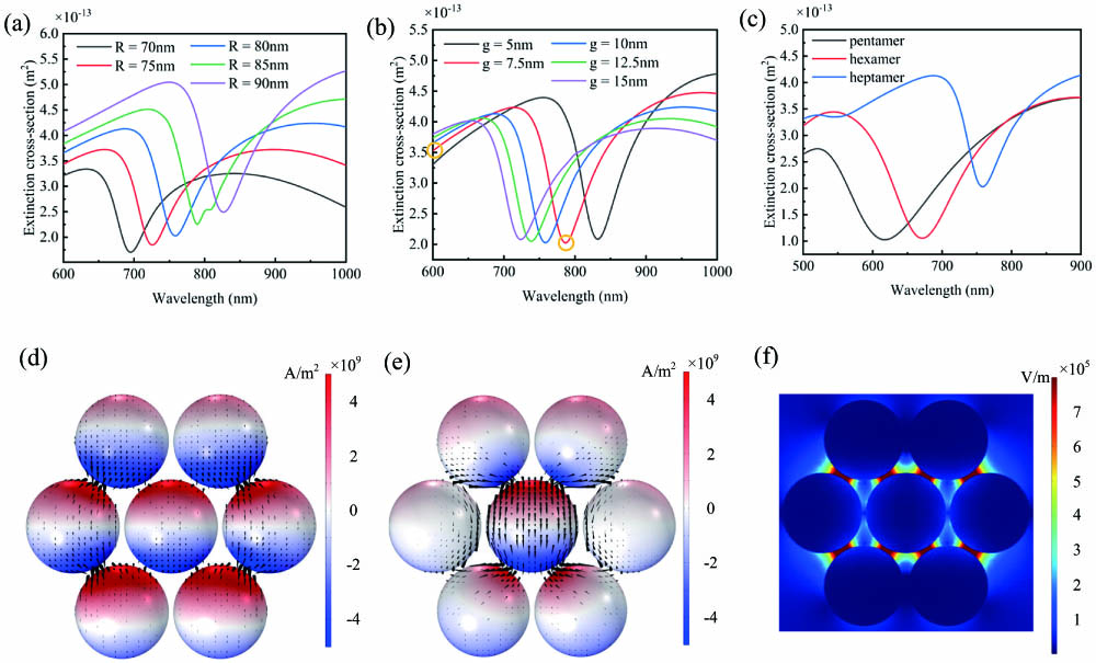
To illustrate the Fano resonance of the oligomer structure, the designed structure was calculated using the finite element method (FEM). The designed heptamer structure is shown in Fig. 5 in Appendix A, where R is the radius of the AuNPs, and g is the distance between the center nanoparticle and the outer ones. Figures 1(a) and 1(b) are the extinction cross-section of the heptamer under different R and g values, respectively. The existence of the Fano dip confirms the generation of Fano resonance. In addition, the position of the Fano dip can be effectively adjusted by changing the radius of the nanoparticles and the spacing between the nanoparticles. By changing the radius from 70 nm to 90 nm, the Fano resonance wavelength can be adjusted from 700 nm to 830 nm. By changing the spacing from 5 nm to 15 nm, the Fano resonance wavelength can be adjusted from 830 nm to 720 nm. To improve the responsivity of the photodetector in the near-infrared wavelength regime, a heptamer with a radius of 80 nm and spacing of 7.5 nm is adopted to generate strong Fano resonance at 785 nm. By changing the number of nanoparticles, other oligomers can be formed, such as hexamer and pentamer, as shown in Fig. 5 (Appendix A).
Figure 1.(a) Effect of changing nanoparticle size on the Fano resonance dip position. (b) Effect of changing nanoparticle spacing on the Fano resonance dip position. (c) Effect of changing the number of particles (heptamer, hexamer, and pentamer) on the Fano resonance dip position. (d) Surface current density and displacement current distribution (arrows) at 600 nm. (e) Surface current density and displacement current distribution (arrows) at the Fano dip wavelength (785 nm). (f) Calculated normalized electric field distribution of the heptamer structure.
Figure 1(c) shows the extinction cross-sections of heptamers, hexamers, and pentamers. As the number of particles decreases, the Fano resonance wavelength of the hexamers and pentamers gradually blue shifted to 620 nm and 670 nm, respectively. To study the Fano resonance mechanism of the heptamer, the surface charge distribution at wavelengths of 600 nm and 785 nm [circles in Fig. 1(b)] are calculated. Figure 1(d) shows the surface current density at the wavelength of 600 nm. The seven nanoparticles oscillate in phase, which originated from the interference between light directly coupled to a bright mode. Figure 1(e) shows the surface current density at 785 nm. The central nanoparticle and six surrounding nanoparticles oscillate in different phases and form two displacement current loops, which indicates the emergence of the dark mode. The destructive coupling between the bright mode and dark mode in the near field results in the enhancement of the maximum electromagnetic field at 785 nm, which can be confirmed by the strong electric “hot” spots between the central sphere and the surrounding spheres in Fig. 1(f).
The scheme of the photodetector is shown in Fig. 2(a). The AuNPs oligomers were assembled in a nanohole array on the silicon substrate and covered with few-layered , and the electrodes were prepared on the two ends of the . To fabricate the photodetector, a nanohole array with specific sizes was prepared on the silicon substrate using the electron beam lithography process. The fabricated nanohole array can be seen in Fig. 7 in Appendix B, and the diameter of the nanohole was . The oligomer structures were assembled in the nanohole array using the CAPA process (Fig. 8 in Appendix B). With the designed nanohole spatial confinement and the AuNPs each with a diameter of 160 nm, many heptamers were assembled inside the nanoholes. Some other oligomers such as hexamer and pentamer were also assembled in the nanoholes due to the size variation of the nanohole and AuNPs during fabrication and synthesis processes, as shown in Fig. 9 in Appendix B; mechanically exfoliated few-layered was transferred to the nanohole arrayed silicon substrate. Finally, electrodes were prepared at both ends of using photolithography and magnetron sputtering. Figure 2(b) shows the scanning electron microscopy (SEM) image of the prepared photodetector with oligomer structures, and the electrodes are mounted at both ends of the . The flake has an area of . There were oligomers covered by the flake; of them were heptamers, hexamers, and pentamers (Appendix B). For comparison, a photodetector without an oligomer structure was fabricated as a control, and the SEM image is shown in Fig. 2(c). The Raman spectra of the in both devices are shown in Fig. 2(d); two characteristic peaks of the can be seen at and 408 nm. Note that the positions of the two peaks are shifted compared to that of the monolayer , which is consistent with the case of the few-layer [36]. In addition, under the same test conditions, the Raman intensity of the photodetector with oligomer structures was seven times higher than that of the control group, which indicates a strong electric field enhancement generated by Fano resonance. For this photodetector, there is a Schottky barrier at the contact between the gold oligomers and the . When light illuminates on the oligomers, the Fano resonance generates hot electrons which have higher energy than the Schottky barrier. Thus, the hot electrons can be emitted from the gold oligomers to the , resulting in hot electron injection [Fig. 2(e)] [37]. Figure 2(f) shows the energy band diagram of the heterojunction [18]. Under light illumination, the heterojunction absorbs photons to generate carriers. The carriers drifted under bias voltage and created a photocurrent; together with the hot electron injection, this generates a strong photocurrent.
Figure 2.(a) Schematic of the photodetector. (b) SEM image of the photodetector. (c) SEM images of the photodetectors of the control group. (d) Raman spectra of the on devices. (e) Schematic illustration of the internal photoemission in the Schottky junction. (f) Energy band diagram of .
The photocurrent characteristics of the fabricated photodetector are measured using laser diodes and a Keithley 2601 source meter. The diameter of the laser spot is , which can fully cover the photodetector. Figure 3 shows the current−voltage (I-V) relation of the device under different optical powers at different wavelengths. The black curve represents the dark current of the device measured in the dark state. With the bias varied between and 3 V, the dark currents are changed in a range with a magnitude of μ. Because the increase in the optical power excites a larger number of photo-generated carriers, a stronger photocurrent can be generated under a bias voltage. It can be seen that a much greater photocurrent of the device is generated compared to the dark current, which is proportional to the absorbed optical power. The photocurrent increases with the bias voltage, which reaches a maximum at the bias of 3 V. As the larger bias voltage was applied, more photo-generated carriers drifted to the electrodes, resulting in an increased photocurrent. The device has a response at a light wavelength ranging from 450 nm to 1064 nm. It is found that at 785 nm, the device exhibits the strongest light response under 785 nm illumination, and its photocurrent magnitude is about two orders of magnitude higher than that of no illumination, as shown in Fig. 3(d). Most of the oligomers assembled are heptamers, which generate Fano resonance at incident light with a 785 nm wavelength. The strong electromagnetic field induced by Fano resonance created many hot electrons on the surface of the nanoparticles, which cross the Schottky barrier and are injected into the . Under the bias voltage, the injected free carriers drifted to electrodes and lead to a strong current.
Figure 3.I-V characteristic curves of devices at (a) 450 nm, (b) 520 nm, (c) 635 nm, (d) 785 nm, and (e) 1064 nm, respectively.
We further evaluated the responsivity (R) and detectivity () of the photodetectors, which are described by where is the current under illumination, is the dark current, is the incident light intensity, is the effective area, and is the absolute value of the electron charge ().
Figure 4(a) shows the responsivity and detectivity calculated under 785 nm illumination and 3 V bias. Note that the responsivity of the device decreases with an increase in the optical power, which resulted from the saturation of the trap states either in the or the interface [38]. Note that our devices have the highest responsivity and detection rate under an incident light power of 5.3 mW, which is up to 52 A/W and Jones, respectively. To evaluate the dynamic response of the photodetector, we measured its impulse response. Figure 4(b) is the I-T response curve of the device measured with a bias voltage of 3 V. The incident light intensity is 33.8 mW with a wavelength of 785 nm, from which it can be seen that the prepared device presented a typical photodiode switching behavior depending on the laser on/off state. Furthermore, the rise and fall times of the device were measured by an oscilloscope. The test results show that the response time of the device is less than 0.6 ms, demonstrating its fast response and high sensitivity. Figure 4(c) shows the responsivity of our device compared to the control group (tested with a 785 nm light source with 3 V bias); the control device has a responsivity of 13 A/W and a detection rate of Jones under the same conditions. Note that the responsivity of the proposed device is about four times that of the control group.
Figure 4.(a) Responsivity and detectivity of the device at different optical powers. (b) I-T response of the proposed device. (c) Comparison of the responsivity of the device and the control.
In summary, we demonstrated a Fano resonance-enhanced heterojunction photodetector, which is enabled by the internal hot-electron injection process in the gold oligomers– junction. By integrating a flake on a silicon substrate with an oligomer array and aligning two Au electrodes on two ends of the flake, the oligomers generate a strong Fano resonance upon incident light. Hot electrons are generated on the oligomers and transferred to the channel above due to the low Au− Schottky barrier, which yields a considerable photocurrent. A photoresponsivity of 52 A/W is obtained at a wavelength of 785 nm with a bias of 3 V, while the detection rate reaches Jones. The photodetector has a fast response speed; the rise and fall time is less than 0.6 ms. The demonstrated Fano resonance-enhanced heterojunction photodetector outperforms other heterojunction photodetectors, especially in the near-infrared regime. The performance of similar photodetectors is summarized in Table 1. Our research breaks the limitations of conventional enhancement with gold nanoparticles and will provide an idea for future research on the use of gold nanoparticles to enhance the near-infrared light band.
Performance Comparison of Photodetector-Based MoS
Device
R (A/W)
D (Jones)
(nm)
References
heterojunction
52
785
This work
heterojunction
0.3
808
[19]
heterojunction
11.9
650
[20]
heterojunction
9
550
[21]
heterojunction
76.1
660
[18]
Monolayer phototransistor
880
/
561
[38]
Few-layer phototransistor
0.57
532
[3]
APPENDIX A: SIMULATION
In the simulation, a 3D model of nano oligomers (Fig. 5) is established for calculation, and the top and bottom boundaries of the model are set as input ports and output ports, respectively. For the input port, a plane wave propagating in the z direction with an electric field polarized in the y direction was used during the study. The extinction spectrum is represented by the extinction cross section
Figure 5.(a) Heptamer structure. R is the radius of AuNPs, and g is the distance between the central nanoparticles and the surrounding nanoparticles. (b) Schematic diagram of the hexamer. (c) Schematic diagram of the pentamer.
In these equations, is the intensity of the incident light, n represents the normal vector pointing outward from the oligomer structure, corresponds to the scattering intensity vector, and Q stands for the power loss density. The integration in Eq. (A2) is taken as its volume. The integration in Eq. (A3) is performed on the scattered closed surface. A perfectly matched layer (PML) is placed around the nanostructures to prevent reflected light fields.
APPENDIX B: PREPARATION AND CHARACTERIZATION
The Au oligomers were then assembled using capillary-assisted particle assembly (CAPA) method on the prepared substrate. The prepared hole diameter on the substrate is , and AuNPs with a diameter of 160 nm were adopted in the assembly. With the geometric size constraints, certain types of oligomers such as heptamers, hexamers, and pentamers can be assembled in the holes. Figure 8(a) shows the schematic of the CAPA method. Here is a detailed description of the CAPA process. The hole array silicon substrate and a piece of quartz glass with a thickness of 1 mm were ultrasonically cleaned in acetone solution, anhydrous ethanol, and deionized water for 480 s, respectively. 0.1 mg/mL, 300 μL of AuNPs were centrifuged at 2000 r/min for 3 min. After centrifugation, the supernatant was removed, and the remaining 30 μL of concentrated solution was taken out for CAPA. The hole array substrate was plasma treated to increase the hydrophilicity of the surface, and it was fixed on the heat plate with double-sided adhesive tape. The concentrated AuNPs solution was dripped on the substrate, and the quartz glass was fixed at 700 μm above the silicon substrate by a motorized XYZ stage to control the AuNPs droplets. The heat plate was set at 40°C above the dew point temperature. The stage was moved parallel to the substrate with a displacement speed at 5 μm/s to assemble the AuNPs into the holes. After assembly, adhesive tape was used to remove the excess AuNPs on the surface of the substrate. Figures 8(b)–8(d) show the SEM image of 160 nm gold particles assembled by the CAPA method on the silicon substrate without a nanohole array. Note that CAPA can assemble AuNPs with a dense arrangement. The oligomers assembled on the hole array substrate are shown in Figs. 9(a)–9(c). Compared to hole array substrate without AuNPs (Fig. 7 of Appendix B), it can be seen that a large number of oligomers such as heptamers, hexamers, and pentamers were formed in the hole array. To verify that Fano resonance can be generated from these oligomers, we obtained the reflection spectrum of the oligomers on the hole array substrate, as shown in Fig. 10. The spectrum clearly demonstrated that the Fano resonance originated from the oligomers. Due to the large spot size from the microscope, the collected reflection spectrum originated from multiple oligomers (containing heptamers and other types of oligomers), which resulted in a broadened Fano dip compared to the calculated spectrum shown in Fig. 1(c). Finally, a few-layer is stripped from the bulk by mechanical exfoliation and transferred above the oligomer structure under a depth of field microscope. Ni/Au (10 nm/90 nm) electrodes were deposited by photolithography and magnetron sputtering to the two ends of the flake to prepare a photodetector [Fig. 2(b)].
Figure 6.(a) Schematic view of the silicon substrate with a hole array. (b) Silicon substrate with oligomer structures. (c) Substrate with a few layers of transferred above. (d) Two electrodes were prepared on two ends of the . (e) Enlarged view of the oligomer on the device.
[26] N. Ansari, E. Mohebbi. Broadband and high absorption in Fibonacci photonic crystal including MoS2 monolayer in the visible range. J. Phys. D, 51, 115101(2018).