• Photonics Research
  • Vol. 10, Issue 6, 1472 (2022)
Jiachen Li1, Sigang Yang1, Hongwei Chen1, Xingjun Wang2, Minghua Chen1、*, and Weiwen Zou3
Author Affiliations
  • 1Beijing National Research Center for Information Science and Technology (BNRist), Department of Electronic Engineering, Tsinghua University, Beijing 100084, China
  • 2State Key Laboratory of Advanced Optical Communications System and Networks, Department of Electronics, School of Electronics Engineering and Computer Science, Peking University, Beijing 100871, China
  • 3State Key Laboratory of Advanced Optical Communication Systems and Networks, Intelligent Microwave Lightwave Integration Innovation Center (imLic), Department of Electronic Engineering, Shanghai Jiao Tong University, Shanghai 200240, China
  • show less
    DOI: 10.1364/PRJ.452631 Cite this Article Set citation alerts
    Jiachen Li, Sigang Yang, Hongwei Chen, Xingjun Wang, Minghua Chen, Weiwen Zou. Fully integrated hybrid microwave photonic receiver[J]. Photonics Research, 2022, 10(6): 1472 Copy Citation Text show less
    Packaged FIH-MWPR module with a compact volume of 30 mm×20 mm×10 mm.
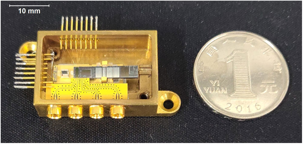
    Fig. 1. Packaged FIH-MWPR module with a compact volume of 30  mm×20  mm×10  mm.
    (a) Schematic diagram of the proposed FIH-MWPR. DFB, distributed feedback semiconductor laser; SSC, spot-size converter; PM, phase modulator; MRR, microring resonator; PD, photodetector. (b) Spectra at several key points labeled in the system. 1, 2, and 3 are optical spectra, and 4 is the electrical spectrum. The signal–signal beat interference (SSBI) at 4 is ignored. (c) Optical microscope images of key elements on the fabricated SOI chip. (d) Cross-sectional schematic view (not to scale) of the SOI platform.
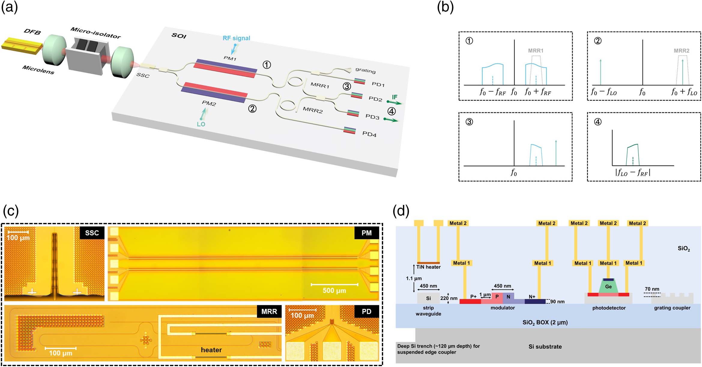
    Fig. 2. (a) Schematic diagram of the proposed FIH-MWPR. DFB, distributed feedback semiconductor laser; SSC, spot-size converter; PM, phase modulator; MRR, microring resonator; PD, photodetector. (b) Spectra at several key points labeled in the system. 1, 2, and 3 are optical spectra, and 4 is the electrical spectrum. The signal–signal beat interference (SSBI) at 4 is ignored. (c) Optical microscope images of key elements on the fabricated SOI chip. (d) Cross-sectional schematic view (not to scale) of the SOI platform.
    Normalized measured E/O modulation responses of (a) the unpackaged on-chip phase modulator and (b) the packaged phase modulator under various bias voltages.
    Fig. 3. Normalized measured E/O modulation responses of (a) the unpackaged on-chip phase modulator and (b) the packaged phase modulator under various bias voltages.
    (a) Measured MRR notch response (green, dots), simulated MRR bandpass response (blue, solid line), and the Lorentzian fitting (green, dashed line) of the measured notch response. (b) The MRR resonance wavelength is tuned with the increasing heating power. (c) Temporal waveform of the square-wave electrical driving signal applied on the TiN microheater. (d) Measured temporal optical response with a fall/rise time of ∼66 and ∼15 μs.
    Fig. 4. (a) Measured MRR notch response (green, dots), simulated MRR bandpass response (blue, solid line), and the Lorentzian fitting (green, dashed line) of the measured notch response. (b) The MRR resonance wavelength is tuned with the increasing heating power. (c) Temporal waveform of the square-wave electrical driving signal applied on the TiN microheater. (d) Measured temporal optical response with a fall/rise time of 66 and 15  μs.
    (a) Measured responsivities of on-chip photodetectors under various bias voltages. (b) Normalized measured O/E responses of on-chip photodetectors under various bias voltages.
    Fig. 5. (a) Measured responsivities of on-chip photodetectors under various bias voltages. (b) Normalized measured O/E responses of on-chip photodetectors under various bias voltages.
    (a) Measured optical spectrum of the employed InP-based DFB semiconductor laser. (b) Frequency noise measurement of the DFB laser showing a Lorentzian linewidth of ∼320 kHz.
    Fig. 6. (a) Measured optical spectrum of the employed InP-based DFB semiconductor laser. (b) Frequency noise measurement of the DFB laser showing a Lorentzian linewidth of 320  kHz.
    (a) Measured electrical spectrum (RBW: 100 kHz, VBW: 1 kHz) of the down-converted IF signal, with the two-tone RF signal centered at 14 GHz (14.001 and 13.999 GHz) and the LO (20 dBm) centered at 14.2 GHz. (b) Measured output power of the IF fundamental tones and the IMD3 tones under different RF input power. (c) Measured link gain of the FIH-MWPR over the frequency range from 2 to 18 GHz. (d) Measured noise floor of the FIH-MWPR over the frequency range from 2 to 18 GHz. (e) Measured NF of the FIH-MWPR over the frequency range from 2 to 18 GHz. (f) Measured SFDR of the FIH-MWPR over the frequency range from 2 to 18 GHz.
    Fig. 7. (a) Measured electrical spectrum (RBW: 100 kHz, VBW: 1 kHz) of the down-converted IF signal, with the two-tone RF signal centered at 14 GHz (14.001 and 13.999 GHz) and the LO (20 dBm) centered at 14.2 GHz. (b) Measured output power of the IF fundamental tones and the IMD3 tones under different RF input power. (c) Measured link gain of the FIH-MWPR over the frequency range from 2 to 18 GHz. (d) Measured noise floor of the FIH-MWPR over the frequency range from 2 to 18 GHz. (e) Measured NF of the FIH-MWPR over the frequency range from 2 to 18 GHz. (f) Measured SFDR of the FIH-MWPR over the frequency range from 2 to 18 GHz.
    Link gain, NF, and SFDR measured as functions of IF. Here, the RF input signal is fixed at 14 GHz, while the LO (20 dBm) is tuned from 14.1 to 17 GHz.
    Fig. 8. Link gain, NF, and SFDR measured as functions of IF. Here, the RF input signal is fixed at 14 GHz, while the LO (20 dBm) is tuned from 14.1 to 17 GHz.
    (a) Experimental setup for evaluating the system performance of the FIH-MWPR as a de-chirp receiver. The inset shows the de-chirping principle. MZM, Mach–Zehnder modulator; EDFA, erbium-doped fiber amplifier; OBPF, optical bandpass filter; OC, optical coupler; VOA, variable optical attenuator; PD, photodetector; AWG, arbitrary waveform generator; LNA, low noise amplifier; EBPF, electrical bandpass filter; ADC, analog to digital converter; DSP, digital signal processor. (b) Instantaneous time-frequency diagrams of generated LFM radar echo signals from the fiber-delay-based radar target emulator at different frequency bands (S-, C-, X-, and Ku-bands). (c) The normalized electrical spectra of de-chirped IF signals generated by the FIH-MWPR, with the LFM radar signals located at different frequency bands (S-, C-, X-, and Ku-bands). The insets show the zoom-in views around the main peaks. (d) Measured frequencies of the de-chirped IF signals under different fiber delay distances, with the LFM radar signals located at different frequency bands (S-, C-, X-, and Ku-bands).
    Fig. 9. (a) Experimental setup for evaluating the system performance of the FIH-MWPR as a de-chirp receiver. The inset shows the de-chirping principle. MZM, Mach–Zehnder modulator; EDFA, erbium-doped fiber amplifier; OBPF, optical bandpass filter; OC, optical coupler; VOA, variable optical attenuator; PD, photodetector; AWG, arbitrary waveform generator; LNA, low noise amplifier; EBPF, electrical bandpass filter; ADC, analog to digital converter; DSP, digital signal processor. (b) Instantaneous time-frequency diagrams of generated LFM radar echo signals from the fiber-delay-based radar target emulator at different frequency bands (S-, C-, X-, and Ku-bands). (c) The normalized electrical spectra of de-chirped IF signals generated by the FIH-MWPR, with the LFM radar signals located at different frequency bands (S-, C-, X-, and Ku-bands). The insets show the zoom-in views around the main peaks. (d) Measured frequencies of the de-chirped IF signals under different fiber delay distances, with the LFM radar signals located at different frequency bands (S-, C-, X-, and Ku-bands).
    PlatformsConfiguration and Integration LevelVolume (cm3)Power Consumption (W)Operation Bandwidth (GHz)Link Gainb(dB)NFb(dB)SFDRb(dB·Hz2/3)
    Hybrid III-V/SOI (this work)All components (laser, modulators, filters, and PDs) are on-chip and hybrid integrated.61.22–18−51.9 to −58.659.7–75.289.0–94.1
    Hybrid III-V/LiNbO3 crystal/fiber [11]Unpackaged laser, crystal modulators, fiber filters, and PDs are hybrid integrated into a common enclosure.180510–1850 (at 18 GHz)55 (at 18 GHz)105 (at 12 GHz)
    SOI [15]Modulators, filters, and PDs are on-chip. The laser is from an external device.N/AN/A2–1050 (at 3 GHz)72 (at 3 GHz)91.9 (at 3 GHz)
    SOI [16]Modulators and PDs are on-chip. The laser is from an external device. No optical filters.N/AN/A3.4–14.159 (at 10.4 GHz)N/A99 (at 10.4 GHz)
    Table 1. Comparison among Reported Integrated Microwave Photonic Receivers [11,15,16]a
    Jiachen Li, Sigang Yang, Hongwei Chen, Xingjun Wang, Minghua Chen, Weiwen Zou. Fully integrated hybrid microwave photonic receiver[J]. Photonics Research, 2022, 10(6): 1472
    Download Citation