
Kapil Debnath, David J. Thomson, Weiwei Zhang, Ali Z. Khokhar, Callum Littlejohns, James Byers, Lorenzo Mastronardi, Muhammad K. Husain, Kouta Ibukuro, Frederic Y. Gardes, Graham T. Reed, Shinichi Saito, "All-silicon carrier accumulation modulator based on a lateral metal-oxide-semiconductor capacitor," Photonics Res. 6, 373 (2018)
- Photonics Research
- Vol. 6, Issue 5, 373 (2018)
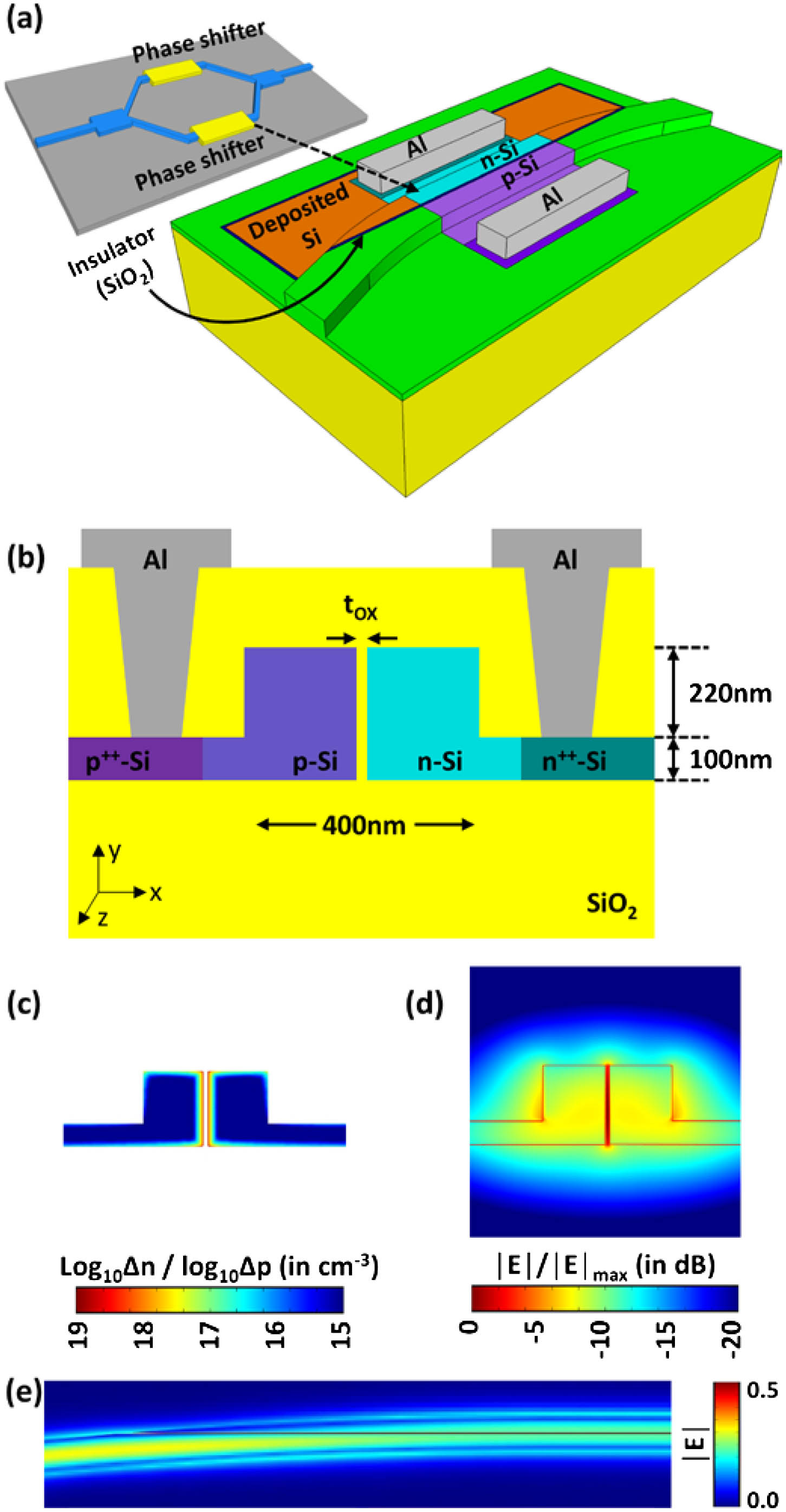
Fig. 1. (a) Schematic of the Si / SiO 2 / Si 1 × 10 18 cm − 3 1 × 10 20 cm − 3 t ox | E x | | E x |
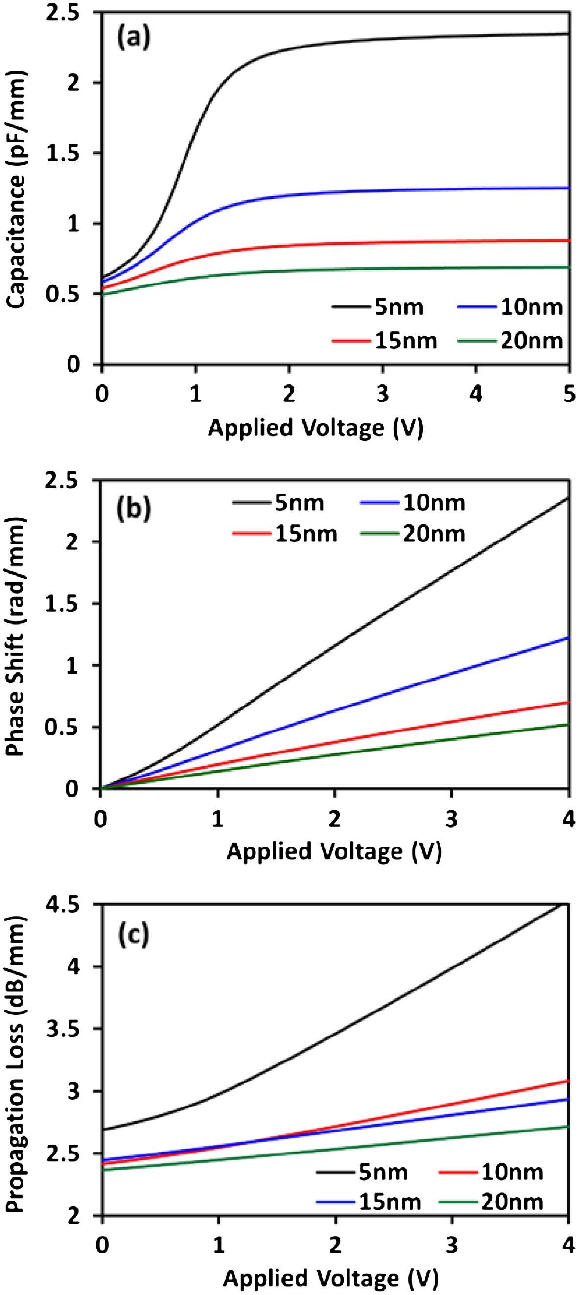
Fig. 2. (a) Calculated change in device capacitance (in pF/mm) as a function of applied voltage. Since the modulator operates in accumulation regime, only positive bias is shown. The capacitance increases with reducing oxide thickness (t ox
Fig. 3. (a) Cross-sectional SEM image of the fabricated modulator across the active region. (b) Magnified view of the MOS capacitor at the rib section, where the oxide layer is clearly visible. (c) Optical image of the fabricated MZI modulator with 500-μm-long phase shifter.
Fig. 4. (a) Measured transmission spectra of the MZI modulator with 500-μm-long phase shifter as a function of applied voltage. The signal probe was connected to n-Si electrode while the ground probe was connected to the p-Si electrode. The output power of the modulator was normalized to a reference Si waveguide with same length. (b) Measured phase modulation (in radian) and extracted modulation efficiency V π L π V · c m 20 Gbit / s 25 Gbit / s


Set citation alerts for the article
Please enter your email address

© Copyright 2018-2021 | Chinese Laser Press. All Rights Reserved 沪ICP备15018463号-20