Abstract
In silicon photonics, the carrier depletion scheme has been the most commonly used mechanism for demonstrating high-speed electro-optic modulation. However, in terms of phase modulation efficiency, carrier-accumulation-based devices potentially offer almost an order of magnitude improvement over those based on carrier depletion. Previously reported accumulation modulator designs only considered vertical metal-oxide-semiconductor (MOS) capacitors, which imposes serious restrictions on the design flexibility and integratability with other photonic components. In this work, for the first time to our knowledge, we report experimental demonstration of an all-silicon accumulation phase modulator based on a lateral MOS capacitor. Using a Mach–Zehnder interferometer modulator with a 500-μm-long phase shifter, we demonstrate high-speed modulation up to with a modulation efficiency () of .1. INTRODUCTION
Over the last four decades, ultra-fast fiber optic networks have dominated long-distance communication systems (e.g., long-haul fiber optic telecom networks) and even most of the data communication networks (e.g., active optical cables). However, for short-reach communications (), e.g., rack-to-rack communication or inter- and intra-chip communications, metal interconnects are still predominantly used. As the demand for higher bandwidth at lower power consumption is increasing, optical interconnection for inter-chip or even chip-scale communication is soon becoming a necessity [1]. This is because metal-based (primarily copper) interconnects are reaching their physical limits due to their prohibitively high energy consumption at higher data rates. Bringing the optical technology closer to the transistors would require high-volume production, scalability, and most importantly opto-electronic integration. In recent years, silicon photonics (SiP) has been identified as the most viable technology for this purpose [2]. The main reasons behind this are the compatibility to complementary-metal-oxide-semiconductor (CMOS) manufacturing processes and the potential for monolithic photonic-electronic integration in the longer term. Transmitting data optically has several advantages: ultra-high aggregate bandwidth [terahertz (THz)], low energy dissipation during transmission (due to the absence of joule heating), inherent parallelism from wavelength division multiplexing, low signal distortion, etc. In silicon (Si) waveguides, transmission at high data rates over [3] has been demonstrated. This suggests that the transmission capacity of a Si-based optical interlink will be mainly determined by the optical modulation and detection speed. Furthermore, fundamentally there is negligible energy dissipation associated with optical data transmission; hence, to realize an energy-efficient optical link, it is vital to reduce energy consumption during modulation and detection operations [4].
Since the inception of SiP technology, there has been a significant amount of research done to realize energy-efficient and high-speed modulators. In silicon, the conventional electro-optic modulation schemes such as the Pockels effect and the Franz–Keldysh effect are either absent or negligibly small. As a result, modulation in Si is primarily realized using the free-carrier-plasma-dispersion effect [5]. There are three modulation schemes that are used to achieve free-carrier-based modulation in Si: (i) carrier injection, (ii) carrier depletion, and (iii) carrier accumulation. Carrier-injection-based modulators, which are based on forward-biased PIN diodes, offer the highest electro-optic modulation efficiency [6]. This helps to realize small and energy-efficient modulators [7,8]. However, the speed of carrier-injection-based devices is limited by the free-carrier lifetime at the junction and the reported speed so far has been limited to a few Gbit/s [7–9], without the use of pre-emphasis techniques. Carrier-depletion-based modulators are realized using reverse-biased PN diodes and can offer very large modulation bandwidths (up to [10]). The fabrication process of the depletion type modulator is also relatively straightforward. As a result, this has largely become the preferred modulation scheme in SiP [10–12]. However, carrier-depletion-based modulators have a much lower modulation efficiency in comparison to carrier-injection-based devices and hence require a large footprint and much higher operating energy [13]. The carrier accumulation scheme offers both high modulation efficiency as well as large modulation bandwidth. This type of modulation is realized using a metal-oxide-semiconductor (MOS)-type capacitor structure incorporated in an optical waveguide. Very high modulation efficiencies with voltage-length product () as small as and a modulation speed up to [14] have been demonstrated. Thus this scheme is very useful in realizing smaller and more energy efficient modulators without having to compromise the modulation speed. In all the previously reported accumulation type modulator designs, the MOS-capacitor typically consisted of a vertical stack of either poly- layers [14–17] or III-V/insulator/Si [18,19]. The vertical stacking was adopted to simplify the fabrication process. However, due to the stacked nature of this design, it also imposes a serious restriction on the design flexibility and integratability with other photonic components. For example, this type of modulator design would require a transition region to couple the optical mode of a passive waveguide to the active modulator section to avoid reflections from the effective index mismatch of the waveguides. This could result in increased insertion loss and a large footprint of such devices. Another major drawback of such a structure is the lack of possibility to incorporate it in different optical devices, such as ring resonators, rib waveguides, and photonic crystal structures, in order to improve device performance and achieve application specific properties. In that sense, it would be far more favorable to design a carrier-accumulation-based modulator with a lateral MOS-capacitor structure in a traditional rib waveguide structure (i.e., with a vertical oxide barrier) [20–22].
In this paper, we report the design and, for the first time, experimental demonstration of an all-Si carrier-accumulation-based MOS-capacitor modulator with a lateral MOS capacitor. The paper is organized as follows. In Section 2, we discuss the architecture of the modulator and how the oxide thickness of the MOS capacitor affects the device performance, such as modulation efficiency and speed. In Section 3, we give details of the fabrication process flow. Here we used a sequential fabrication process to realize an extremely narrow oxide region (14 nm) within an optical waveguide. We also used an epitaxial regrowth process to produce crystalline Si on both sides of the MOS capacitor, eliminating the loss of poly-silicon regions, and hence improving the optical transmission of the device. Finally, in Section 4 we present our experimental results. Using an MOS-capacitor-based Mach–Zehnder interferometer (MZI) modulator, we demonstrate high-speed modulation up to with an extinction ratio of 3.65 dB and modulation efficiency of .
Sign up for Photonics Research TOC. Get the latest issue of Photonics Research delivered right to you!Sign up now
2. MODULATOR ARCHITECTURE AND SIMULATION PERFORMANCE
Here we investigate an MZI-based modulator design with a Si MOS-capacitor phase shifter, as shown in Fig. 1(a), to demonstrate the performance, which can theoretically be achieved by using this device configuration. Figure 1(b) shows the cross-sectional image of the phase shifter. The modulator was designed in a 340-nm silicon-on-insulator (SOI) platform with a 2-μm-thick buried-oxide (BOx) layer. The phase-shifter region of the MZI modulator consisted of a thin insulating () layer sandwiched between two complementary doped Si layers. Both lightly doped n- and p-regions had doping concentrations of to lower electrical access resistance and ensure high-bandwidth performance while maintaining a reasonably low optical loss. The heavily doped regions of doping concentration were used to achieve ohmic contacts with the electrodes and positioned 900 nm away from the center of the waveguide to avoid significant modal overlap and therefore optical loss. The confinement of the optical mode was achieved by using a rib waveguide structure, which also ensured electrical accessibility of the MOS capacitor through the slab regions to either side. When a positive bias is applied to the p-doped region with respect to n-doped region, majority carriers accumulate on both sides of the insulating layer.
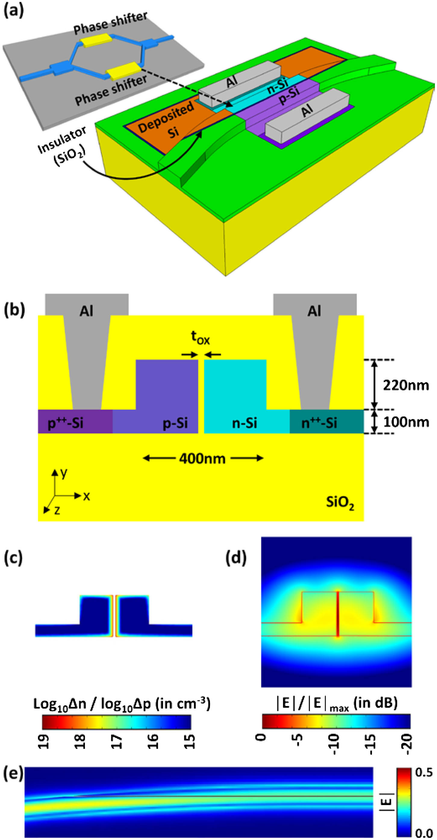
Figure 1.(a) Schematic of the MOS-capacitor phase shifter. The relative position of the phase shift in an MZI interferometer is highlighted in yellow. (b) Cross-sectional view of the MOS-capacitor structure used for designing the phase modulator. The width and height of the rib waveguide are 400 nm and 320 nm, respectively, and the slab height is 100 nm. The n-Si and p-Si regions have a doping concentration of . The n++-Si and p++-Si regions have a doping concentration of and are positioned 900 nm away from the center of the waveguide. The oxide thickness is varied in the design to optimize device performance. (c) Excess carrier concentration distribution (in log scale) due to an applied bias of 4 V. (d) Normalized dominant electric field () profile (in dB) of the fundamental TE mode centered around the oxide slot region. (e) Simulated electric field () propagation from the rib waveguide region to the slot-waveguide region.
A simulated distribution of excess carrier concentration for an applied bias of 4 V is shown in Fig. 1(c). Such a change in free-carrier concentration in Si alters the refractive index and optical absorption around the oxide region, causing a phase change in the propagating optical mode in the rib waveguide. The rib waveguide width was 400 nm to ensure single-mode behavior. The slab region had a thickness of 100 nm to ensure low device access resistance while maintaining a high optical confinement within the rib waveguide region. For the transverse electric (TE) polarization, the optical mode in this waveguide behaves as a slot mode, as shown in Fig. 1(d), which has a strong discontinuity in the electric field at the oxide interfaces. This ensures a strong overlap between the optical mode and the region with accumulated charge carriers. According to our simulations, the planar nature of our modulator design allows us to achieve a seamless transition between the standard rib waveguide mode and the slot mode by gradually introducing the oxide layer within the waveguide as shown in Fig. 1(a). To achieve such low-loss transition, we used a waveguide bend with 50-μm radius. This resulted in a coupling length of less than 5 μm. A 3D finite-difference time-domain (FDTD) simulation suggests a coupling loss of per coupler. Figure 1(e) shows the simulated electric field () propagation from the rib-waveguide region to the slot-waveguide region.
One of the most critical parameters for an accumulation-type modulator is the insulating layer thickness () of the MOS capacitor. Of course, there are several other parameters that also directly or indirectly influence the device performance, such as doping concentration and doping profile, waveguide height and width, and slab thickness. These parameters can be adjusted to further optimize the performance, however, here we mainly study the device performance as a function of the insulating layer thickness while keeping other device parameters constant. Commercially available charge transport solvers (Lumerical DEVICE 6.0 and Silvaco) were used to obtain the carrier concentration profiles and device capacitances for different oxide thicknesses and at different bias voltages. The spatial free-carrier distributions at different bias voltages were then exported to a mode solver (Lumerical MODE Solutions 7.8) for obtaining the phase shift and propagation loss for different oxide thicknesses and bias voltages.
The device capacitance as a function of applied voltage for different oxide thicknesses () is shown in Fig. 2(a). As one would expect, the C-V relationship of this device is similar to a conventional MOS capacitor. There are three operating regimes in an MOS capacitor: accumulation, depletion, and inversion. For the modulation purposes, we are mainly interested in device operation in accumulation mode and avoid the inversion regime, so that the device bandwidth is not limited by carrier recombination in Si. Therefore, only positive bias is shown in the figures. When a positive bias is applied to the p-terminal, the device makes the transition from depletion mode operation towards the accumulation mode, and the device capacitance initially increases upon reaching the “surface accumulation” condition at the flat-band voltage, where it takes a mostly constant value with increasing bias. Analytically, under accumulation, the device capacitance can be expressed as , where is the oxide permittivity, and , , and are the height, thickness, and length of the oxide layer. From this equation we can see that as the oxide thickness reduces, the device capacitance increases. Simulated results also show a monotonic increase in device capacitance as the oxide thickness is reduced from 20 to 5 nm. As the device capacitance increases the electrical relaxation time constant (RC-product) also increases, which degrades the modulation bandwidth. For example, a device with 20 nm oxide can support a modulation bandwidth up to 52 GHz for a voltage swing of 0–4 V, whereas for 5 nm oxide, the modulation bandwidth will reduce to 20 GHz for n- and p-region doping concentration of . Therefore, in order to achieve higher modulation speed a thicker oxide would be preferred. However, modulation bandwidth is not the only key performance indicator of an electro-optic modulator. It is also necessary to achieve a high modulation efficiency. High modulation efficiency ensures shorter devices and/or lower drive voltages and hence low energy consumption and optical loss. The modulation efficiency is directly related to how much accumulation is possible for a given voltage and device length. For a capacitor, the stored charge on both sides of the insulator is given by , where is the voltage across the capacitor. Here we can see that as the capacitance of the device increases, the accumulation capability also increases for the same applied voltage. Therefore, a thinner oxide would give a better modulation efficiency. Figure 2(b) shows the simulated phase shift in a 1-mm-long modulator as a function of applied bias for different oxide thicknesses (). When the oxide thickness is reduced from 20 to 5 nm, the phase shift increases from 0.5 to 2.3 rad. In terms of value, the efficiency improves from 2.40 to . A trade-off therefore exists between device speed and efficiency. Here we would also like to highlight the fact that in the accumulation regime the phase shift with voltage is very linear. Figure 2(c) shows how the propagation loss through the modulator increases with applied voltage and oxide thickness. This is due to the increase in free-carrier concentration. For the experimental demonstration of our designed modulator, we opted for a 10-nm oxide thickness. The motivation behind this was to demonstrate a good compromise of both high-speed operation and good modulation efficiency. From the simulated results, we found that for a device with 10 nm oxide, in accumulation mode, the capacitance is around and the modulation efficiency is about . The modulation bandwidth can reach up to 32 GHz.

Figure 2.(a) Calculated change in device capacitance (in pF/mm) as a function of applied voltage. Since the modulator operates in accumulation regime, only positive bias is shown. The capacitance increases with reducing oxide thickness (). (b) Calculated phase shift (in rad/mm) as a function of applied voltage. The phase shift per unit length increases with reducing oxide thickness and applied voltage. (c) Calculated propagation loss (in dB/mm) as a function of applied voltage. The loss increases with reducing oxide thickness and applied voltage.
3. DEVICE FABRICATION
The proposed modulator structure, shown in Fig. 1(a), was fabricated on a 150 mm SOI wafer with 340-nm-thick top Si layer with 2 μm BOx. The most critical component of our modulator design is the rib waveguide with arbitrarily narrow oxide slot at the center. To realize such a structure, we followed a similar fabrication process that we previously reported in Ref. [23]. We started the fabrication process by creating rectangular trench in the Si overlayer using a combination of ebeam lithography and inductively coupled plasma (ICP) dry etching. The wafer was then annealed at 950°C for 2 min in to grow 10 nm of thermal oxide on the side walls of the trench. Here we selectively removed the thermal oxide from the top of the Si overlayer, while keeping the oxide on the side walls of the trench. A 350-nm-thick amorphous-silicon () layer was then deposited using plasma-enhanced chemical vapor deposition (PECVD). For a good electrical performance, we must transform the amorphous silicon into either crystalline-Si or polycrystalline-silicon (polySi). However, polySi is significantly more optically lossy. Therefore, here we used epitaxial recrystallization to achieve a single crystal layer from the deposited . For this recrystallization, we used the SOI silicon layer as the seed layer and the recrystallization process was initiated from the top surface of the Si overlayer. A detailed discussion on this regrowth process can be found in our previously reported work [23].
After the recrystallization process, the wafer was planarized using chemical mechanical polishing (CMP) to leave a silicon overlayer thickness of 320 nm. Boron and phosphorous ions were then implanted on both sides and 100 nm away from the thin oxide slot region. This was done to avoid any cross-doping and mitigate errors due to misalignment of the lithography process. We then used a thermal diffusion process to target n- and p-doping concentrations of on both sides of the oxide layer. The waveguide layout including MZI structure was then fabricated in the SOI layer using ebeam lithography and dry etching. Here we used an asymmetric MZI design with an arm length mismatch of 200 μm to convert phase modulation into intensity modulation. The highly doped p++ and n++ regions were then implanted to achieve a doping concentration of . It should be noted here that for this first demonstration the doping levels, positions and profiles were not optimized and such design improvements are expected to yield large enhancements in the device performance. After all the doping steps, the device was cladded with a 1-μm-thick PECVD oxide and via holes was etched through the oxide layer on top of the heavily doped regions for metal contacts. Finally, a 1.6-μm-thick metal stack of Ti/TiN/Al/TiN/Ti was sputtered and etched to form the metal electrodes. Here we used a coplanar waveguide (CPW) electrode design to drive the device at high speed.
A cross-sectional scanning electron microscope (SEM) image of the fabricated device is shown in Fig. 3(a). Figure 3(b) shows a close-up view of the rib section of the waveguide. The oxide slot region is clearly visible at the center of the waveguide. Also, we did not observe any poly-silicon grain boundaries around the center of the waveguide. By using epitaxial recrystallization we were able to achieve single crystal Si on both sides of the oxide layer. Figure 3(c) shows an optical image of a fabricated MZI modulator with 500-μm-long active region.
Figure 3.(a) Cross-sectional SEM image of the fabricated modulator across the active region. (b) Magnified view of the MOS capacitor at the rib section, where the oxide layer is clearly visible. (c) Optical image of the fabricated MZI modulator with 500-μm-long phase shifter.
4. CHARACTERIZATION RESULTS
The fabricated MZI modulator was characterized using a fiber-coupled tunable laser source with a tuning range from 1530 to 1630 nm. The polarization of the input light was set to be TE by using a fiber polarization rotator. Coupling of light in and out of the device was achieved by fiber-grating couplers. For DC characterization, the wavelength was scanned using the built-in sweeping ability of the laser, and the detector automatically recorded the output spectra. Figure 4(a) shows the measured transmission spectra at different applied voltages across one of the modulator arms. The transmission spectra were normalized to a standard rib waveguide of the same length in order to remove measurement system losses. Transmission minima in the spectrum of the asymmetric MZI, with an arm length mismatch of 200 μm, had a free spectral range (FSR) of 2.6 nm. Precise characterization of the losses for this first fabrication run was hindered by variation in performance across the chip, and here we present a worst case. The extinction ratio of the MZI structure is approximately 20 dB, and the total insertion loss at the transmission peak was about 26 dB. From a cut-back loss measurement of a test structure containing identical active regions to that in the device, we found that the active region had an insertion loss of , whereas the same waveguides but without doping showed a loss of . This suggests that the loss due to doping was about . Therefore, for our modulator with 500-μm-long active regions, the propagation loss due to the phase modulator was 2.5 dB and the rest of the optical loss of about 23.5 dB was due to the passive structure, which consists of the MMIs, waveguide bends, and standard waveguide-slot waveguide coupling regions. Moreover, analysis of passive test structure suggests that the fabricated rib to slot waveguides are giving much higher losses () as compared to our simulated value (), which we expect is due to an imperfection in our fabrication process. These losses are unexpectedly high and can be significantly improved by further design and process optimization. When a positive bias is applied to the p-terminal of the phase modulator in one of the arms of the MZI modulator, the free carriers start to accumulate around the oxide layer, causing a decrease in the effective index of the biased MZI arm. This results in a blueshift of the MZI transmission spectrum, as can be seen in Fig. 4(a). The modulation efficiency of our device was analyzed by observing the amount of shift in the spectral response of the asymmetric MZI due to applied bias voltage. This spectral shift can be converted to phase shift by relating it to the FSR of the asymmetric MZI spectra. The phase shift of our 500-μm-long modulator as a function of applied voltage is shown in Fig. 4(b) with red circles. The modulation efficiency , which is defined as the voltage-length product for a -radian phase shift, is also estimated from the phase shift and plotted in Fig. 4(b) with green squares as a function of applied voltage. The phase shift and modulation efficiency are calculated in all cases with respect to 0 V. For an electro-optic modulator, the lower the value, the better the performance in terms of device footprint and energy consumption. We also notice that is not fixed and reduces with applied bias as expected from the simulation. At an operating voltage of 6 V, which we used for high-speed analysis, the value is . According to our simulation, this corresponds to an oxide slot thickness of 14 nm.
Figure 4.(a) Measured transmission spectra of the MZI modulator with 500-μm-long phase shifter as a function of applied voltage. The signal probe was connected to n-Si electrode while the ground probe was connected to the p-Si electrode. The output power of the modulator was normalized to a reference Si waveguide with same length. (b) Measured phase modulation (in radian) and extracted modulation efficiency (in ) as a function of applied voltage. (c) Measured eye diagrams at and . In all cases the driving voltage was 6 V with a DC bias of 3 V.
High-speed analysis was performed by observing the device’s modulation ability at different data rates. For this a pseudorandom binary sequence (PRBS) source was used to provide the input signal. A commercial drive amplifier was then used to boost the amplitude to 6 V peak-to-peak before passing the signal through a bias tee, to provide a 3-V DC bias level, ensuring the voltage applied to the device remained positive and therefore in the accumulation regime. The signal was then applied to the device through the use of a high-speed ground-signal-ground (GSG) probe, which contacted the input pad of the coplanar waveguide electrode leading to the phase modulator in one of the MZI arms. At the output pad of the CPW electrode a second GSG probe was used to provide a DC block and termination. The operating wavelength was then set to 1558.8 nm, which corresponds to the quadrature point of the asymmetric MZI spectral response. Output light collected from the device was passed to an erbium-doped fiber amplifier (EDFA) to boost the optical power and optical filter and to partially remove noise generated by the EDFA. The light was then passed to the DCA for analysis of the optical eye diagram. Open eye diagrams were observed up to . Figure 4(c) shows eye diagrams at and with extinction ratios of 3.7 dB and 3.6 dB, respectively. The measured eye diagram indicates a modulation bandwidth which is smaller than what we have predicted from our simulation, i.e., 42 GHz. One possible reason for reduced bandwidth could be the additional contact resistance of , which was not considered while calculating the device bandwidth. Also the device resistance was slightly higher due to lower doping concentration, which was achieved as compared to that targeted and used for our simulation. The actual doping concentrations in the rib are estimated to be around instead of through analysis of the electrical characteristics of PN diode test structures on the same wafer.
5. CONCLUSION
In conclusion, we successfully demonstrated for the first time a carrier accumulation modulator in Si using a lateral MOS capacitor. The modulator was realized in a 340-nm SOI platform. We observed an open eye diagram for bit rate up to with extinction ratio of 3.65 dB. At the driving voltage of 6 V the modulation efficiency was measured to be . To reduce the propagation loss through the active waveguide region, we also implemented an epitaxial recrystallization process. As a result, the propagation loss through the active region was 2.5 dB.
Although for this first demonstration only a modest performance has been achieved, our simulations have shown that with design and process optimization the performance can be competitive as compared to the vertical stack approach. The lateral device configuration can also be advantageous from a design flexibility perspective, allowing the implementation of ring-resonator- and photonic-crystal-based modulators as well as ease of integration with photonic circuits based upon traditional strip and rib waveguides. Such a device can therefore be promising for the next generation of low-power photonic modulators.
Acknowledgment
Acknowledgment. University of Southampton Zepler Institute Research Collaboration Stimulus Fund, and Hitachi. G. T. Reed is a Royal Society Wolfson Merit Award holder and is grateful to both the Royal Society and the Wolfson Foundation for funding the award. D. J. Thomson acknowledges funding from the Royal Society for his University Research Fellowship. All data supporting this study are available upon request from the University of Southampton repository at http://doi.org/10.5258/SOTON/D0305.
References
[1] D. A. B. Miller. Rationale and challenges for optical interconnects to electronic chips. Proc. IEEE, 88, 728-749(2000).
[2] R. Soref. Silicon photonics: a review of recent literature. Silicon, 2, 1-6(2010).
[3] B. G. Lee, X. Chen, A. Biberman, X. Liu, I.-W. Hsieh, C.-Y. Chou, J. I. Dadap, F. Xia, W. M. J. Green, L. Sekaric, Y. A. Vlasov, R. M. Osgood, K. Bergman. Ultrahigh-bandwidth silicon photonic nanowire waveguides for on-chip networks. IEEE Photon. Technol. Lett., 20, 398-400(2008).
[4] D. A. B. Miller. Attojoule optoelectronics for low-energy information processing and communications. J. Lightwave Technol., 35, 346-396(2017).
[5] R. A. Soref, B. R. Bennett. Electrooptical effects in silicon. IEEE J. Quantum Electron., 23, 123-129(1987).
[6] W. M. Green, M. J. Rooks, L. Sekaric, Y. A. Vlasov. Ultra-compact, low RF power, 10 Gb/s silicon Mach-Zehnder modulator. Opt. Express, 15, 17106-17113(2007).
[7] Q. Xu, B. Schmidt, S. Pradhan, M. Lipson. Micrometre-scale silicon electro-optic modulator. Nature, 435, 325-327(2005).
[8] K. Debnath, L. O’Faolain, F. Y. Gardes, A. G. Steffan, G. T. Reed, T. F. Krauss. Cascaded modulator architecture for WDM applications. Opt. Express, 20, 27420-27428(2012).
[9] K. Preston, S. Manipatruni, A. Gondarenko, C. B. Poitras, M. Lipson. Deposited silicon high-speed integrated electro-optic modulator. Opt. Express, 17, 5118-5124(2009).
[10] X. Xiao, M. Li, L. Wang, D. Chen, Q. Yang, S. Yu. High speed silicon photonic modulators. Optical Fiber Communications Conference and Exhibition (OFC), 1-3(2017).
[11] D. J. Thomson, F. Y. Gardes, Y. Hu, G. Mashanovich, M. Fournier, P. Grosse, J.-M. Fedeli, G. T. Reed. High contrast 40 Gbit/s optical modulation in silicon. Opt. Express, 19, 11507-11516(2011).
[12] D. Thomson, F. Gardes, J. Fedeli, S. Zlatanovic, Y. Hu, B. Kuo, E. Myslivets, N. Alic, S. Radic, G. Z. Mashanovich, G. T. Reed. 50 Gbit/s silicon optical modulator. IEEE Photon. Technol. Lett., 24, 234-236(2012).
[13] G. T. Reed, G. Mashanovich, F. Y. Gardes, D. J. Thomson. Silicon optical modulators. Nat. Photonics, 4, 518-526(2010).
[14] M. Webster, P. Gothoskar, V. Patel, D. Piede, S. Anderson, R. Tummidi, D. Adams, C. Appel, P. Metz, S. Sunder, B. Dama, K. Shastri. An efficient MOS-capacitor based silicon modulator and CMOS drivers for optical transmitters. IEEE 11th International Conference on Group IV Photonics (GFP), 1-2(2014).
[15] A. Liu, R. Jones, L. Liao, D. Samara-Rubio, D. Rubin, O. Cohen, R. Nicolaescu, M. Paniccia. A high-speed silicon optical modulator based on a metal-oxide-semiconductor capacitor. Nature, 427, 615-618(2004).
[16] J. Fujikata, S. Takahashi, M. Takahashi, M. Noguchi, T. Nakamura, Y. Arakawa. High-performance MOS-capacitor-type Si optical modulator and surface-illumination-type Ge photodetector for optical interconnection. Jpn. J. Appl. Phys., 55, 04EC01(2016).
[17] M. Sodagar, A. H. Hosseinnia, P. Isautier, H. Moradinejad, S. Ralph, A. A. Eftekhar, A. Adibi. Compact, 15 Gb/s electro-optic modulator through carrier accumulation in a hybrid Si/SiO2/Si microdisk. Opt. Express, 23, 28306-28315(2015).
[18] J. H. Han, F. Boeuf, J. Fujikata, S. Takahashi, S. Takagi, M. Takenaka. Efficient low-loss InGaAsP/Si hybrid MOS optical modulator. Nat. Photonics, 11, 486-490(2017).
[19] T. Hiraki, T. Aihara, K. Hasebe, K. Takeda, T. Fujii, T. Kakitsuka, T. Tsuchizawa, H. Fukuda, S. Matsuo. Heterogeneously integrated III-V/Si MOS capacitor Mach-Zehnder modulator. Nat. Photonics, 11, 482-485(2017).
[20] M. Douix, D. Marris-Morini, C. Baudot, S. Crémer, D. Rideau, D. Perez-Galacho, A. Souhaite, R. Blanc, E. Batail, N. Vulliet, L. Vivien, E. Cassan, F. Boeuf. Design of integrated capacitive modulators for 56 Gbps operation. IEEE 13th International Conference on Group IV Photonics (GFP), 5-7(2016).
[21] A. Abraham, O. Dubray, S. Olivier, D. Marrls-Morini, S. Menezo, L. Vivien. Low-voltage and low-loss silicon modulator based on carrier accumulation using a vertical slot waveguide. IEEE 14th International Conference on Group IV Photonics (GFP), 118-119(2016).
[22] D. Perez-Galacho, A. Abraham, S. Olivier, L. Vivien, D. Marris-Morini. Silicon modulator based on interleaved capacitors in subwavelength grating waveguides. Proc. SPIE, 9891, 989112(2016).
[23] K. Debnath, A. Z. Khokhar, G. T. Reed, S. Saito. Fabrication of arbitrarily narrow vertical dielectric slots in silicon waveguides. IEEE Photon. Technol. Lett., 29, 1269-1272(2017).


